FDS6675BZ Fairchild Optoelectronics Group, FDS6675BZ Datasheet - Page 2
FDS6675BZ
Manufacturer Part Number
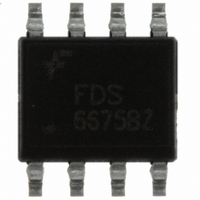
FDS6675BZ
Description
MOSFET P-CH 30V 8-SOIC
Manufacturer
Fairchild Optoelectronics Group
Series
PowerTrench®r
Datasheet
1.FDS6675BZ.pdf
(6 pages)
Specifications of FDS6675BZ
Fet Type
MOSFET P-Channel, Metal Oxide
Fet Feature
Logic Level Gate
Rds On (max) @ Id, Vgs
13 mOhm @ 11A, 10V
Drain To Source Voltage (vdss)
30V
Current - Continuous Drain (id) @ 25° C
11A
Vgs(th) (max) @ Id
3V @ 250µA
Gate Charge (qg) @ Vgs
62nC @ 10V
Input Capacitance (ciss) @ Vds
2470pF @ 15V
Power - Max
1W
Mounting Type
Surface Mount
Package / Case
SO-8
Lead Free Status / RoHS Status
Lead free / RoHS Compliant
Other names
FDS6675BZTR
Available stocks
Company
Part Number
Manufacturer
Quantity
Price
Company:

Part Number:
FDS6675BZ
Manufacturer:
FSC
Quantity:
10 000
Company:
Part Number:
FDS6675BZ
Manufacturer:
FAIRCHILD
Quantity:
40 045
Part Number:
FDS6675BZ
Manufacturer:
FSC
Quantity:
20 000
Part Number:
FDS6675BZ-NL
Manufacturer:
FAIRCHILD/仙童
Quantity:
20 000
Part Number:
FDS6675BZ_NL
Manufacturer:
ON/安森美
Quantity:
20 000


©2009 Fairchild Semiconductor Corporation
FDS6675BZ Rev.B2
Electrical Characteristics
Off Characteristics
On Characteristics
Dynamic Characteristics
Switching Characteristics
Drain-Source Diode Characteristics
Notes:
1: R
2: Pulse Test:Pulse Width <300 us, Duty Cycle < 2.0%
3: The diode connected between the gate and source serves only as protection against ESD. No gate overvoltage rating is implied.
B
∆B
I
I
V
r
g
C
C
C
t
t
t
t
Q
Q
Q
Q
V
t
Q
DSS
GSS
∆V
d(on)
r
d(off)
f
rr
DS(on)
FS
VDSS
GS(th)
SD
iss
oss
rss
∆T
∆T
g
g
gs
gd
rr
drain pins. R
Symbol
VDSS
θJA
GS(th)
Scale 1 : 1 on letter size paper
J
J
is the sum of the junction-to-case and case-to-ambient thermal resistance where the case thermal reference is defined as the solder mounting surface of the
θJC
Drain to Source Breakdown Voltage
Breakdown Voltage Temperature
Coefficient
Zero Gate Voltage Drain Current
Gate to Source Leakage Current
Gate to Source Threshold Voltage
Gate to Source Threshold Voltage
Temperature Coefficient
Drain to Source On Resistance
Forward Transconductance
Input Capacitance
Output Capacitance
Reverse Transfer Capacitance
Turn-On Delay Time
Rise Time
Turn-Off Delay Time
Fall Time
Total Gate Charge
Total Gate Charge
Gate to Source Gate Charge
Gate to Drain Charge
Source to Drain Diode Forward Voltage V
Reverse Recovery Time
Reverse Recovery Charge
is guaranteed by design while R
(Note 2)
a) 50°C/W when
mounted on a 1 in
pad of 2 oz copper
Parameter
(Note 2)
θCA
T
is determined by the user’s board design.
J
2
= 25°C unless otherwise noted
I
I
25°C
V
V
V
I
25°C
V
V
V
T
V
V
f = 1MHz
V
V
V
I
V
I
I
D
D
D
D
I
F
F
J
D
DS
GS
GS
GS
GS
GS
DS
DS
DD
GS
DS
DS
GS
= -11A
= -11A, di/dt = 100A/µs
= -11A, di/dt = 100A/µs
= -250µA, V
= -250µA, referenced to
= -250µA, referenced to
= 125
= -11A
= -5V,
= -15V, V
= -15V, V
= -24V, V
= -15V, V
= 0V, I
= ±25V, V
= V
= -10V , I
= -4.5V, I
= -10V, I
= -15V, I
= -10V, R
2
Test Conditions
DS
b)105°C/W when
mounted on a .04 in
pad of 2 oz copper
o
C
, I
S
= -2.1A
D
D
D
I
D
GS
GS
D
GS
D
GS
GS
GS
DS
= -11A
= -11A
= -250µA
= -9A
= -11A
= -11A
= -10V,
= -5V,
= 0V
= 0V,
= 6Ω
= 0V
= 0V
2
Min
-30
-1
1855
15.7
10.8
17.4
15.0
11.4
Typ
335
330
120
-0.7
-20
3.0
7.8
7.2
34
60
44
25
-2
minimun pad
c) 125°C/W when
mounted on a
www.fairchildsemi.com
2470
Max
13.0
21.8
18.8
±10
450
500
200
100
-1.2
10
16
62
35
42
30
-1
-3
mV/°C
mV/°C
Units
mΩ
µA
µA
pF
pF
pF
nC
nC
nC
nC
nC
ns
ns
ns
ns
ns
V
V
S
V
Related parts for FDS6675BZ
Image
Part Number
Description
Manufacturer
Datasheet
Request
R

Part Number:
Description:
LED 7-SEG SGL CC RED RHDP .3"
Manufacturer:
Fairchild Optoelectronics Group
Datasheet:

Part Number:
Description:
LED IR EMITTING 940NM SIDELOOKER
Manufacturer:
Fairchild Optoelectronics Group
Datasheet:

Part Number:
Description:
LED IR EMITTING GAAS 940NM 3MM
Manufacturer:
Fairchild Optoelectronics Group
Datasheet:
Part Number:
Description:
LED IR EMITTING ALGAAS 880NM 3MM
Manufacturer:
Fairchild Optoelectronics Group
Datasheet:
Part Number:
Description:
LED IR EMITTING 940NM SMD 2MM
Manufacturer:
Fairchild Optoelectronics Group
Datasheet:
Part Number:
Description:
IC PHOTOTRANS IR 940NM BLK 1.9MM
Manufacturer:
Fairchild Optoelectronics Group
Datasheet:
Part Number:
Description:
LED IR GAAS SIDELOOK 940NM
Manufacturer:
Fairchild Optoelectronics Group
Datasheet:
Part Number:
Description:
LED IR EMITTING 940NM 2MM SMD
Manufacturer:
Fairchild Optoelectronics Group
Datasheet:
Part Number:
Description:
IC PHOTOTRANS IR 940NM 1.9MM GW
Manufacturer:
Fairchild Optoelectronics Group
Datasheet:
Part Number:
Description:
LED IR EMITTING 880NM 2-PLCC
Manufacturer:
Fairchild Optoelectronics Group
Datasheet:
Part Number:
Description:
LED 7-SEG SGL CC RED RHDP .3"
Manufacturer:
Fairchild Optoelectronics Group
Datasheet:

Part Number:
Description:
DIODE EMITTING GAAS IRED TO-46
Manufacturer:
Fairchild Optoelectronics Group
Datasheet:
Part Number:
Description:
DIODE EMITTING GAAS IRED TO-46
Manufacturer:
Fairchild Optoelectronics Group
Datasheet:

Part Number:
Description:
LED SS BIPO RED/GRN DIFF PCB 5MM
Manufacturer:
Fairchild Optoelectronics Group
Datasheet:

Part Number:
Description:
LED SS HI EFF GREEN DIFF 3MM
Manufacturer:
Fairchild Optoelectronics Group
Datasheet: