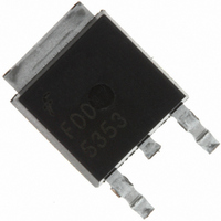
FDD5353 Fairchild Semiconductor, FDD5353 Datasheet
首页 Discrete Semiconductor Products MOSFETs, GaNFETs - Single FDD5353
Manufacturer Part Number
FDD5353
Description
MOSFET N-CH 60V 11.5A DPAK
Manufacturer
Fairchild Semiconductor
Specifications of FDD5353
Fet Type
MOSFET N-Channel, Metal Oxide
Fet Feature
Logic Level Gate
Rds On (max) @ Id, Vgs
12.3 mOhm @ 10.7A, 10V
Drain To Source Voltage (vdss)
60V
Current - Continuous Drain (id) @ 25° C
11.5A
Vgs(th) (max) @ Id
3V @ 250µA
Gate Charge (qg) @ Vgs
65nC @ 10V
Input Capacitance (ciss) @ Vds
3215pF @ 30V
Power - Max
3.1W
Mounting Type
Surface Mount
Package / Case
DPak, TO-252 (2 leads+tab), SC-63
Configuration
Single
Transistor Polarity
N-Channel
Resistance Drain-source Rds (on)
0.0123 Ohm @ 10 V
Drain-source Breakdown Voltage
60 V
Gate-source Breakdown Voltage
+/- 20 V
Continuous Drain Current
11.5 A
Power Dissipation
3100 mW
Maximum Operating Temperature
+ 150 C
Mounting Style
SMD/SMT
Minimum Operating Temperature
- 55 C
Lead Free Status / RoHS Status
Lead free / RoHS Compliant
Available stocks
©2008 Fairchild Semiconductor Corporation
FDD5353 Rev.C
FDD5353
N-Channel Power Trench
60V, 50A, 12.3mΩ
Features
MOSFET Maximum Ratings
Thermal Characteristics
Package Marking and Ordering Information
V
V
I
E
P
T
R
R
D
DS
GS
AS
D
J
θJC
θJA
Max r
Max r
100% UIL Tested
RoHS Compliant
, T
Symbol
Device Marking
STG
FDD5353
DS(on)
DS(on)
= 12.3mΩ at V
= 15.4mΩ at V
Drain to Source Voltage
Gate to Source Voltage
Drain Current -Continuous (Package limited)
Single Pulse Avalanche Energy
Power Dissipation
Power Dissipation
Operating and Storage Junction Temperature Range
Thermal Resistance, Junction to Case
Thermal Resistance, Junction to Ambient
G
S
GS
GS
= 10V, I
= 4.5V, I
-Continuous
-Continuous (Silicon limited)
-Pulsed
FDD5353
Device
(TO -252)
D -PA K
TO -2 52
D
D
= 10.7A
= 9.5A
T
C
®
= 25°C unless otherwise noted
MOSFET
Parameter
D
D-PAK (TO-252)
Package
1
T
T
T
T
T
General Description
This
Semiconductor‘s advanced Power Trench
been especially tailored to minimize the on-state resistance and
yet maintain superior switching performance.
Application
A
C
C
A
C
= 25°C
= 25°C
= 25°C
= 25°C
= 25°C
Inverter
Synchronous rectifier
Primary switch
N-Channel
Reel Size
13’’
G
(Note 1a)
(Note 1a)
(Note 1a)
(Note 3)
MOSFET
Tape Width
D
S
is
12mm
-55 to +150
Ratings
produced using Fairchild
11.5
±20
100
253
1.8
3.1
60
50
54
69
40
®
process that has
www.fairchildsemi.com
March 2008
2500 units
Quantity
Units
°C/W
mJ
°C
W
V
V
A
tm
Related parts for FDD5353
FDD5353 Summary of contents
... Thermal Resistance, Junction to Case θJC R Thermal Resistance, Junction to Ambient θJA Package Marking and Ordering Information Device Marking Device FDD5353 FDD5353 ©2008 Fairchild Semiconductor Corporation FDD5353 Rev.C ® MOSFET General Description = 10.7A This N-Channel D Semiconductor‘s advanced Power Trench = 9.5A D been especially tailored to minimize the on-state resistance and yet maintain superior switching performance ...
... R is determined by the user’s board design. θJC θJA 2: Pulse Test: Pulse Width < 300µs, Duty cycle < 2.0%. ° 3: Starting 3mH 13A ©2008 Fairchild Semiconductor Corporation FDD5353 Rev 25°C unless otherwise noted J Test Conditions I = 250µ 250µA, referenced to 25° ...
... Figure 3. Normalized On- Resistance vs Junction Temperature 100 µ PULSE DURATION = 80 s DUTY CYCLE = 0.5%MAX 150 GATE TO SOURCE VOLTAGE (V) GS Figure 5. Transfer Characteristics ©2008 Fairchild Semiconductor Corporation FDD5353 Rev 25°C unless otherwise noted J 3.0 = 10V 2.5 2 3.5V GS 1.5 µ 100 125 150 ...
... Switching Capability 200 100 10 THIS AREA IS LIMITED BY r DS(on) 1 SINGLE PULSE T = MAX RATED 1.8 θ 0.1 0 DRAIN to SOURCE VOLTAGE (V) DS Figure 11. Forward Bias Safe Operating Area ©2008 Fairchild Semiconductor Corporation FDD5353 Rev 25°C unless otherwise noted J 10000 = 20V DD 1000 V = 30V DD = 40V ...
... DUTY CYCLE-DESCENDING ORDER D = 0.5 0.1 0.2 0.1 0.05 0.02 0.01 0.01 0.001 0.0001 - ©2008 Fairchild Semiconductor Corporation FDD5353 Rev 25°C unless otherwise noted 1.8 C/W θ RECTANGULAR PULSE DURATION (sec) Figure 13. Transient Thermal Response Curve SINGLE PULSE C/W θ Note 1b ...
... Product Status Advance Information Formative or In Design Preliminary First Production No Identification Needed Full Production Obsolete Not In Production ©2008 Fairchild Semiconductor Corporation FDD5353 Rev.C FPS™ PDP-SPM™ F-PFS™ Power-SPM™ ® FRFET PowerTrench SM Global Power Resource Programmable Active Droop™ ...
Related keywords
FDD5353 datasheet FDD5353 data sheet FDD5353 pdf datasheet FDD5353 component FDD5353 part FDD5353 distributor FDD5353 RoHS FDD5353 datasheet download


