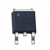
FDD2670 Fairchild Semiconductor, FDD2670 Datasheet - Page 4

FDD2670
Manufacturer Part Number
FDD2670
Description
MOSFET N-CH 200V 3.6A D-PAK
Manufacturer
Fairchild Semiconductor
Series
PowerTrench®r
Datasheet
1.FDD2670.pdf
(5 pages)
Specifications of FDD2670
Fet Type
MOSFET N-Channel, Metal Oxide
Fet Feature
Standard
Rds On (max) @ Id, Vgs
130 mOhm @ 3.6A, 10V
Drain To Source Voltage (vdss)
200V
Current - Continuous Drain (id) @ 25° C
3.6A
Vgs(th) (max) @ Id
4.5V @ 250µA
Gate Charge (qg) @ Vgs
43nC @ 10V
Input Capacitance (ciss) @ Vds
1228pF @ 100V
Power - Max
1.3W
Mounting Type
Surface Mount
Package / Case
DPak, TO-252 (2 leads+tab), SC-63
Transistor Polarity
N Channel
Continuous Drain Current Id
3.6A
Drain Source Voltage Vds
200V
On Resistance Rds(on)
130mohm
Rds(on) Test Voltage Vgs
10V
Threshold Voltage Vgs Typ
4V
Rohs Compliant
Yes
Configuration
Single
Resistance Drain-source Rds (on)
0.13 Ohms
Forward Transconductance Gfs (max / Min)
15 S
Drain-source Breakdown Voltage
200 V
Gate-source Breakdown Voltage
+/- 20 V
Continuous Drain Current
3.6 A
Power Dissipation
3.2 W
Maximum Operating Temperature
+ 150 C
Mounting Style
SMD/SMT
Minimum Operating Temperature
- 55 C
Lead Free Status / RoHS Status
Lead free / RoHS Compliant
Available stocks
Company
Part Number
Manufacturer
Quantity
Price
Part Number:
FDD2670
Manufacturer:
FAIRCHILD/ن»™ç«¥
Quantity:
20 000
Typical Characteristics
15
12
0.001
9
6
3
0
0.01
100
Figure 9. Maximum Safe Operating Area.
0.1
10
0
Figure 7. Gate Charge Characteristics.
1
0.1
0.01
0.1
I
D
R
SINGLE PULSE
R
1
= 3.6 A
DS(ON)
0.001
V
T
JA
5
GS
A
= 96
= 25
LIMIT
= 10V
o
o
C/W
C
10
D = 0.5
0.2
0.1
0.05
0.02
0.01
V
1
DS
, DRAIN-SOURCE VOLTAGE (V)
Q
g
15
, GATE CHARGE (nC)
SINGLE PULSE
0.01
DC
20
10
10s
Figure 11. Transient Thermal Response Curve.
1s
Thermal characterization performed using the conditions described in Note 1b.
Transient thermal response will change depending on the circuit board design.
100ms
V
25
DS
= 40V
10ms
30
100
100 s
100 V
0.1
35
70
V
1000
40
t
1
, TIME (sec)
2000
1500
1000
100
1
500
80
60
40
20
0
0.01
0
Figure 8. Capacitance Characteristics.
0
Figure 10. Single Pulse Maximum
C
ISS
C
OSS
0.1
20
V
Power Dissipation.
C
DS
RSS
, DRAIN TO SOURCE VOLTAGE (V)
10
1
40
t
1
, TIME (sec)
10
60
P(pk)
100
SINGLE PULSE
Duty Cycle, D = t
R
T
R
J
JA
T
R
A
JA
- T
= 96°C/W
= 25°C
(t) = r(t) + R
JA
100
A
t
1
80
= 96°C/W
= P * R
t
FDD2670 Rev C1(W)
2
V
f = 1MHz
GS
= 0 V
JA
1
1000
(t)
JA
/ t
100
2
1000


