IRFR9310TRL Vishay, IRFR9310TRL Datasheet
IRFR9310TRL
Specifications of IRFR9310TRL
Available stocks


Related parts for IRFR9310TRL


IRFR9310TRL Summary of contents
Page 1
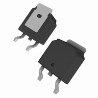
... The straight lead version (IRFU/SiHFU series) is for through-hole P-Channel MOSFET mounting applications. Power dissipation levels up to 1.5 W are possible in typical surface mount applications. DPAK (TO-252) DPAK (TO-252) a IRFR9310TRLPbF IRFR9310TRPbF a SiHFR9310TL-E3 SiHFR9310T- IRFR9310TRL IRFR9310TR a a SiHFR9310TL SiHFR9310T = 25 °C, unless otherwise noted ° 100 ° ...
Page 2
... IRFR9310, IRFU9310, SiHFR9310, SiHFU9310 Vishay Siliconix THERMAL RESISTANCE RATINGS PARAMETER Maximum Junction-to-Ambient Maximum Junction-to-Ambient a (PCB Mount) Maximum Junction-to-Case (Drain) Note a. When mounted on 1" square PCB (FR-4 or G-10 material). SPECIFICATIONS °C, unless otherwise noted J PARAMETER Static Drain-Source Breakdown Voltage V Temperature Coefficient DS Gate-Source Threshold Voltage ...
Page 3
... Document Number: 91284 S-82992-Rev. B, 12-Jan-09 IRFR9310, IRFU9310, SiHFR9310, SiHFU9310 Vishay Siliconix www.vishay.com 3 ...
Page 4
... IRFR9310, IRFU9310, SiHFR9310, SiHFU9310 Vishay Siliconix TYPICAL CHARACTERISTICS 25 °C, unless otherwise noted 10 VGS TOP -15V -10V -8.0V -7.0V -6.0V -5.5V -5.0V BOTTOM -4.5V 1 -4.5V 20μs PULSE WIDTH 0 Drain-to-Source Voltage (V) DS Fig Typical Output Characteristics 10 VGS TOP -15V -10V -8.0V -7.0V -6.0V -5 ...
Page 5
... Fig Typical Gate Charge vs. Gate-to-Source Voltage Document Number: 91284 S-82992-Rev. B, 12-Jan-09 IRFR9310, IRFU9310, SiHFR9310, SiHFU9310 C SHORTED ds 0.1 100 Fig Typical Source-Drain Diode Forward Voltage 100 10 SEE FIGURE 13 0 Vishay Siliconix 10 ° 150 ° 1.0 2.0 3.0 4.0 -V ,Source-to-Drain Voltage (V) SD OPERATION IN THIS AREA LIMITED ...
Page 6
... IRFR9310, IRFU9310, SiHFR9310, SiHFU9310 Vishay Siliconix 2.0 1.6 1.2 0.8 0.4 0 100 T , Case Temperature ( C) C Fig Maximum Drain Current vs. Case Temperature 0.50 1 0.20 0.10 0.05 0.02 SINGLE PULSE 0.1 0.01 (THERMAL RESPONSE) 0.01 0.00001 0.0001 Fig Maximum Effective Transient Thermal Impedance, Junction-to-Case www ...
Page 7
... V 300 TOP 250 BOTTOM 200 150 100 100 Starting T , Junction Temperature ( C) J Fig. 12c - Maximum Avalanche Energy vs. Drain Current Vishay Siliconix Fig. 12b - Unclamped Inductive Waveforms I D -0.49A -0.7A -1.1A 125 150 ° Current regulator Same type as D.U.T. 50 kΩ ...
Page 8
... Inductor current * V Vishay Siliconix maintains worldwide manufacturing capability. Products may be manufactured at one of several qualified locations. Reliability data for Silicon Technology and Package Reliability represent a composite of all qualified locations. For related documents such as package/tape drawings, part marking, and reliability data, see www.vishay.com/ppg?91284. ...
Page 9
... Vishay disclaims any and all liability arising out of the use or application of any product described herein or of any information provided herein to the maximum extent permitted by law. The product specifications do not expand or otherwise modify Vishay’ ...