SUM85N15-19-E3 Vishay, SUM85N15-19-E3 Datasheet - Page 2
SUM85N15-19-E3
Manufacturer Part Number
SUM85N15-19-E3
Description
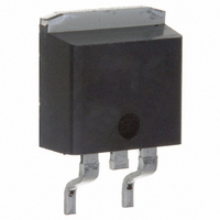
MOSFET N-CH 150V 85A D2PAK
Manufacturer
Vishay
Series
TrenchFET®r
Datasheet
1.SUM85N15-19-E3.pdf
(6 pages)
Specifications of SUM85N15-19-E3
Transistor Polarity
N-Channel
Fet Type
MOSFET N-Channel, Metal Oxide
Fet Feature
Standard
Rds On (max) @ Id, Vgs
19 mOhm @ 30A, 10V
Drain To Source Voltage (vdss)
150V
Current - Continuous Drain (id) @ 25° C
85A
Vgs(th) (max) @ Id
4V @ 250µA
Gate Charge (qg) @ Vgs
110nC @ 10V
Input Capacitance (ciss) @ Vds
4750pF @ 25V
Power - Max
3.75W
Mounting Type
Surface Mount
Package / Case
D²Pak, TO-263 (2 leads + tab)
Minimum Operating Temperature
- 55 C
Configuration
Single
Resistance Drain-source Rds (on)
0.019 Ohm @ 10 V
Forward Transconductance Gfs (max / Min)
25 S
Drain-source Breakdown Voltage
150 V
Gate-source Breakdown Voltage
+/- 20 V
Continuous Drain Current
85 A
Power Dissipation
3750 mW
Maximum Operating Temperature
+ 175 C
Mounting Style
SMD/SMT
Continuous Drain Current Id
85A
Drain Source Voltage Vds
150V
On Resistance Rds(on)
19mohm
Rds(on) Test Voltage Vgs
10V
Threshold Voltage Vgs Typ
2V
Power Dissipation Pd
3.75W
Lead Free Status / RoHS Status
Lead free / RoHS Compliant
Lead Free Status / RoHS Status
Lead free / RoHS Compliant, Lead free / RoHS Compliant
Other names
SUM85N15-19-E3TR
Available stocks
Company
Part Number
Manufacturer
Quantity
Price
Company:

Part Number:
SUM85N15-19-E3
Manufacturer:
HITACHI
Quantity:
1 928
Company:
Part Number:
SUM85N15-19-E3
Manufacturer:
VISHAY
Quantity:
30 000


SUM85N15-19
Vishay Siliconix
Notes
a.
b.
c.
www.vishay.com
2
SPECIFICATIONS (T
Static
Drain-Source Breakdown Voltage
Gate-Threshold Voltage
Gate-Body Leakage
Zero Gate Voltage Drain Current
On-State Drain Current
Drain-Source On-State Resistance
Forward Transconductance
Dynamic
Input Capacitance
Output Capacitance
Reverse Transfer Capacitance
Total Gate Charge
Gate-Source Charge
Gate-Drain Charge
Gate Resistance
Turn-On Delay Time
Rise Time
Turn-Off Delay Time
Fall Time
Source-Drain Diode Ratings and Characteristics (T
Continuous Current
Pulsed Current
Forward Voltage
Reverse Recovery Time
Peak Reverse Recovery Current
Reverse Recovery Charge
Pulse test; pulse width v 300 ms, duty cycle v 2%.
Guaranteed by design, not subject to production testing.
Independent of operating temperature.
c
c
b
g
Parameter
a
c
c
c
c
c
a
a
a
J
=25_C UNLESS OTHERWISE NOTED)
Symbol
V
I
RM(REC)
V
r
(BR)DSS
I
DS(on)
DS(on)
t
t
I
I
C
GS(th)
D(on)
C
C
V
Q
Q
d(on)
d(off)
GSS
DSS
DSS
I
Q
Q
g
R
SM
I
t
oss
t
rss
t
SD
iss
S
rr
fs
gs
gd
r
f
g
rr
g
C
V
V
I
V
V
V
V
D
DS
DS
= 25_C)
GS
GS
GS
DS
DS
^ 85 A, V
= 150 V, V
= 150 V, V
I
= 75 V, V
= 10 V, I
= 10 V, I
V
= 0 V, V
F
V
V
V
V
V
V
DS
V
V
DS
DS
= 50 A, di/dt = 100 A/ms
DS
Test Condition
DD
DD
I
DS
GS
DS
F
= 85 A, V
= 0 V, V
= V
= 150 V, V
w 5 V, V
= 75 V, R
= 75 V, R
= 0 V, I
,
b
= 10 V, I
= 15 V, I
GEN
DS
D
D
GS
GS
GS
GS
GS
= 30 A, T
= 30 A, T
= 25 V, f = 1 MHz
, I
= 10 V, R
GS
= 0 V, T
= 0 V, T
D
= 10 V, I
D
GS
GS
D
= 250 mA
D
L
L
= 250 mA
GS
= "20 V
= 30 A
= 0.9 W
= 0.9 W
= 30 A
= 10 V
= 0 V
= 0 V
,
J
J
J
J
= 125_C
= 175_C
D
D
g
= 125_C
= 175_C
= 2.5 W
= 85 A
Min
150
120
0.5
25
2
0.015
Typ
4750
0.52
530
220
170
170
130
1.8
1.0
76
21
26
22
40
8
S-32523—Rev. B, 08-Dec-03
Document Number: 71703
"100
Max
0.019
0.038
0.050
250
110
250
250
180
200
3.0
1.5
1.2
50
35
60
85
12
4
1
Unit
nA
mA
m
pF
nC
mC
ns
ns
ns
W
W
V
V
A
S
A
A
V
A
Related parts for SUM85N15-19-E3
Image
Part Number
Description
Manufacturer
Datasheet
Request
R

Part Number:
Description:
357-036-542-201 CARDEDGE 36POS DL .156 BLK LOPRO
Manufacturer:
Vishay
Datasheet:
Part Number:
Description:
357-036-542-201 CARDEDGE 36POS DL .156 BLK LOPRO
Manufacturer:
Vishay
Datasheet:
Part Number:
Description:
357-036-542-201 CARDEDGE 36POS DL .156 BLK LOPRO
Manufacturer:
Vishay
Datasheet:
Part Number:
Description:
357-036-542-201 CARDEDGE 36POS DL .156 BLK LOPRO
Manufacturer:
Vishay
Datasheet:
Part Number:
Description:
357-036-542-201 CARDEDGE 36POS DL .156 BLK LOPRO
Manufacturer:
Vishay
Datasheet:
Part Number:
Description:
357-036-542-201 CARDEDGE 36POS DL .156 BLK LOPRO
Manufacturer:
Vishay
Datasheet:
Part Number:
Description:
357-036-542-201 CARDEDGE 36POS DL .156 BLK LOPRO
Manufacturer:
Vishay
Datasheet:
Part Number:
Description:
357-036-542-201 CARDEDGE 36POS DL .156 BLK LOPRO
Manufacturer:
Vishay
Datasheet:
Part Number:
Description:
357-036-542-201 CARDEDGE 36POS DL .156 BLK LOPRO
Manufacturer:
Vishay
Datasheet:
Part Number:
Description:
357-036-542-201 CARDEDGE 36POS DL .156 BLK LOPRO
Manufacturer:
Vishay
Datasheet:
Part Number:
Description:
357-036-542-201 CARDEDGE 36POS DL .156 BLK LOPRO
Manufacturer:
Vishay
Datasheet:
Part Number:
Description:
357-036-542-201 CARDEDGE 36POS DL .156 BLK LOPRO
Manufacturer:
Vishay
Datasheet:
Part Number:
Description:
357-036-542-201 CARDEDGE 36POS DL .156 BLK LOPRO
Manufacturer:
Vishay
Datasheet:
Part Number:
Description:
357-036-542-201 CARDEDGE 36POS DL .156 BLK LOPRO
Manufacturer:
Vishay
Datasheet: