FDA50N50 Fairchild Semiconductor, FDA50N50 Datasheet

MOSFET N-CH 500V 48A TO-3P

FDA50N50

Manufacturer Part Number
FDA50N50
Description
MOSFET N-CH 500V 48A TO-3P
Manufacturer
Fairchild Semiconductor
Series
UniFET™r
Datasheet

Specifications of FDA50N50

Fet Type
MOSFET N-Channel, Metal Oxide
Fet Feature
Standard
Rds On (max) @ Id, Vgs
105 mOhm @ 24A, 10V
Drain To Source Voltage (vdss)
500V
Current - Continuous Drain (id) @ 25° C
48A
Vgs(th) (max) @ Id
5V @ 250µA
Gate Charge (qg) @ Vgs
137nC @ 10V
Input Capacitance (ciss) @ Vds
6460pF @ 25V
Power - Max
625W
Mounting Type
Through Hole
Package / Case
TO-3PN-3
Configuration
Single
Transistor Polarity
N-Channel
Resistance Drain-source Rds (on)
0.105 Ohms
Drain-source Breakdown Voltage
500 V
Gate-source Breakdown Voltage
+/- 20 V
Continuous Drain Current
48 A
Power Dissipation
625 W
Maximum Operating Temperature
+ 150 C
Mounting Style
Through Hole
Minimum Operating Temperature
- 55 C
Lead Free Status / RoHS Status
Lead free / RoHS Compliant

Available stocks

Company
Part Number
Manufacturer
Quantity
Price
Part Number:
FDA50N50
Manufacturer:
FSC
Quantity:
450
Part Number:
FDA50N50
Manufacturer:
FAIRCHILD
Quantity:
102
Part Number:
FDA50N50
Manufacturer:
VISHAY
Quantity:
2 000
Part Number:
FDA50N50
Manufacturer:
ST
0
Part Number:
FDA50N50
Manufacturer:
FAIRCHILD/仙童
Quantity:
20 000
Company:
Part Number:
FDA50N50
Quantity:
9 000
Company:
Part Number:
FDA50N50
Quantity:
20 200
©2008 Fairchild Semiconductor Corporation
FDH50N50_F133 / FDA50N50 Rev. A
FDH50N50_F133 / FDA50N50
500V N-Channel MOSFET
Features
• 48A, 500V, R
• Low gate charge ( typical 105 nC)
• Low C
• Fast switching
• 100% avalanche tested
• Improved dv/dt capability
Absolute Maximum Ratings
Thermal Characteristics
V
I
I
V
E
I
E
dv/dt
P
T
T
R
R
R
D
DM
AR
J,
L
DSS
GSS
AS
AR
D
Symbol
Symbol
θJC
θCS
θJA
T
STG
rss
( typical 45 pF)
G
DS(on)
D
Drain-Source Voltage
Drain Current
Drain Current
Gate-Source voltage
Single Pulsed Avalanche Energy
Avalanche Current
Repetitive Avalanche Energy
Peak Diode Recovery dv/dt
Power Dissipation
Maximum Lead Temperature for Soldering Purpose,
1/8” from Case for 5 Seconds
Thermal Resistance, Junction-to-Case
Thermal Resistance, Case-to-Sink
Thermal Resistance, Junction-to-Ambient
Operating and Storage Temperature Range
S
= 0.105Ω @V
TO-247
FDH Series
GS
- Continuous (T
- Continuous (T
- Pulsed
(T
- Derate above 25°C
= 10 V
Parameter
Parameter
C
= 25°C)
C
C
= 25°C)
= 100°C)
G
D
S
1
Description
These N-Channel enhancement mode power field effect transis-
tors are produced using Fairchild’s proprietary, planar stripe,
DMOS technology.
This advanced technology has been especially tailored to mini-
mize on-state resistance, provide superior switching perfor-
mance, and withstand high energy pulse in the avalanche and
commutation mode. These devices are well suited for high effi-
cient switched mode power supplies and active power factor
correction.
(Note 2)
(Note 1)
(Note 1)
(Note 3)
(Note 1)
FDH50N50_F133/FDA50N50
TO-3PN
FDA Series
Min.
0.24
--
--
-55 to +150
1868
30.8
62.5
500
192
±20
625
300
4.5
48
48
5
G
Max.
0.2
40
--
UniFET
October 2008
S
D
www.fairchildsemi.com
Unit
°C/W
°C/W
°C/W
Unit
W/°C
V/ns
mJ
mJ
°C
°C
W
V
A
A
A
V
A
TM

Related parts for FDA50N50

FDA50N50 Summary of contents

Page 1

... Thermal Resistance, Case-to-Sink θCS R Thermal Resistance, Junction-to-Ambient θJA ©2008 Fairchild Semiconductor Corporation FDH50N50_F133 / FDA50N50 Rev. A Description = 10 V These N-Channel enhancement mode power field effect transis- tors are produced using Fairchild’s proprietary, planar stripe, DMOS technology. This advanced technology has been especially tailored to mini- ...

Page 2

... Starting ≤ 48A, di/dt ≤ 200A/μs, V ≤ Starting DSS 4. Pulse Test: Pulse width ≤ 300μs, Duty Cycle ≤ Essentially Independent of Operating Temperature Typical Characteristics FDH50N50_F133 / FDA50N50 Rev. A Package Reel Size TO-247 - TO-3PN - T = 25°C unless otherwise noted C Conditions 250μ ...

Page 3

... I , Drain Current [A] D Figure 5. Capacitance Characteristics 12,000 10,000 8,000 6,000 4,000 2,000 C rss Drain-Source Voltage [V] DS FDH50N50_F133 / FDA50N50 Rev. A Figure 2. Transfer Characteristics 100 10 1 Notes : 1. 250 μ s Pulse Test 0 Figure 4. Body Diode Forward Voltage 160 120 = 10V 20V GS 40 ...

Page 4

... Drain-Source Voltage [V] DS Figure 11. Typical Drain Current Slope vs. Gate Resistance 4,000 3,500 3,000 2,500 di/dt(on) 2,000 1,500 di/dt(off) 1,000 500 Gate resistance [ G FDH50N50_F133 / FDA50N50 Rev. A (Continued) Figure 8. On-Resistance Variation 2.5 2.0 1.5 1.0 Notes : 0 250 μ 0.0 100 150 200 -100 o C] Figure 10 ...

Page 5

... Typical Performance Characteristics Figure 13. Typical Switching Losses vs. Gate Resistance 1,000 800 600 400 200 Gate resistance [ G Figure 15. Transient Thermal Resistance Curve FDH50N50_F133 / FDA50N50 Rev. A (Continued) Figure 14. Unclamped Inductive Switching 100 Eoff 10 Eon Notes : 400 25A 125 0.01 Ω ] D=0.5 -1 0.2 Notes : ...

Page 6

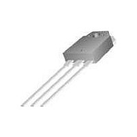
... Mechanical Dimensions FDH50N50_F133 / FDA50N50 Rev. A TO-247AB 6 Dimensions in Millimeters www.fairchildsemi.com ...

Page 7

... Mechanical Dimensions FDH50N50_F133 / FDA50N50 Rev. A TO-3PN 7 Dimensions in Millimeters www.fairchildsemi.com ...

Page 8

... Datasheet Identification Product Status Advance Information Formative / In Design Preliminary First Production No Identification Needed Full Production Obsolete Not In Production FDH50N50_F133 / FDA50N50 Rev. A ® FRFET Programmable Active Droop™ SM ® Global Power Resource QFET Green FPS™ QS™ Green FPS™ e-Series™ ...

Related keywords