HUF75652G3 Fairchild Semiconductor, HUF75652G3 Datasheet
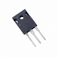
MOSFET N-CH 100V 75A TO-247

HUF75652G3

Manufacturer Part Number
HUF75652G3
Description
MOSFET N-CH 100V 75A TO-247
Manufacturer
Fairchild Semiconductor
Series
UltraFET™r
Type
Power MOSFETr
Datasheet

Specifications of HUF75652G3

Fet Type
MOSFET N-Channel, Metal Oxide
Fet Feature
Logic Level Gate
Rds On (max) @ Id, Vgs
8 mOhm @ 75A, 10V
Drain To Source Voltage (vdss)
100V
Current - Continuous Drain (id) @ 25° C
75A
Vgs(th) (max) @ Id
4V @ 250µA
Gate Charge (qg) @ Vgs
475nC @ 20V
Input Capacitance (ciss) @ Vds
7585pF @ 25V
Power - Max
515W
Mounting Type
Through Hole
Package / Case
TO-247-3
Number Of Elements
1
Polarity
N
Channel Mode
Enhancement
Drain-source On-res
0.008Ohm
Drain-source On-volt
100V
Gate-source Voltage (max)
±20V
Drain Current (max)
75A
Power Dissipation
515W
Output Power (max)
Not RequiredW
Frequency (max)
Not RequiredMHz
Noise Figure
Not RequireddB
Power Gain
Not RequireddB
Drain Efficiency
Not Required%
Operating Temp Range
-55C to 175C
Operating Temperature Classification
Military
Mounting
Through Hole
Pin Count
3 +Tab
Package Type
TO-247
Configuration
Single
Transistor Polarity
N-Channel
Resistance Drain-source Rds (on)
0.008 Ohms
Drain-source Breakdown Voltage
100 V
Gate-source Breakdown Voltage
+/- 20 V
Continuous Drain Current
75 A
Maximum Operating Temperature
+ 175 C
Mounting Style
Through Hole
Minimum Operating Temperature
- 55 C
Lead Free Status / RoHS Status
Lead free / RoHS Compliant

Available stocks

Company
Part Number
Manufacturer
Quantity
Price
Part Number:
HUF75652G3
Manufacturer:
IR
Quantity:
6 000
Part Number:
HUF75652G3
Manufacturer:
Fairchi/ON
Quantity:
48 000
Part Number:
HUF75652G3
Manufacturer:
FSC
Quantity:
20 000
©2001 Fairchild Semiconductor Corporation
75A, 100V, 0.008 Ohm, N-Channel
UltraFET® Power MOSFET
Packaging
Symbol
Absolute Maximum Ratings
Drain to Source Voltage (Note 1) . . . . . . . . . . . . . . . . . . . . . . . . . . . . . . . . . . . . . . . . . . . . . . . V
Drain to Gate Voltage (R
Gate to Source Voltage . . . . . . . . . . . . . . . . . . . . . . . . . . . . . . . . . . . . . . . . . . . . . . . . . . . . . . . V
Drain Current
Pulsed Avalanche Rating . . . . . . . . . . . . . . . . . . . . . . . . . . . . . . . . . . . . . . . . . . . . . . . . . . . . . . UIS
Power Dissipation (Note 2) . . . . . . . . . . . . . . . . . . . . . . . . . . . . . . . . . . . . . . . . . . . . . . . . . . . . . P
Operating and Storage Temperature . . . . . . . . . . . . . . . . . . . . . . . . . . . . . . . . . . . . . . . . . T
Maximum Temperature for Soldering
NOTES:
CAUTION: Stresses above those listed in “Absolute Maximum Ratings” may cause permanent damage to the device. This is a stress only rating and operation of the
device at these or any other conditions above those indicated in the operational sections of this specification is not implied.
All Fairchild semiconductor products are manufactured, assembled and tested under ISO9000 and QS9000 quality systems certification.
1. T
Pulsed Drain Current . . . . . . . . . . . . . . . . . . . . . . . . . . . . . . . . . . . . . . . . . . . . . . . . . . . . . . . . I
Derate Above 25
Leads at 0.063in (1.6mm) from Case for 10s . . . . . . . . . . . . . . . . . . . . . . . . . . . . . . . . . . . . . . . T
Package Body for 10s, See Techbrief TB334. . . . . . . . . . . . . . . . . . . . . . . . . . . . . . . . . . . . . T
Continuous (T
Continuous (T
J
= 25
DRAIN
(TAB)
Product reliability information can be found at http://www.fairchildsemi.com/products/discrete/reliability/index.html
o
C to 150
C
C
o
= 25
= 100
C . . . . . . . . . . . . . . . . . . . . . . . . . . . . . . . . . . . . . . . . . . . . . . . . . . . . . . . . . . . .
o
C.
GS
o
G
C, V
o
JEDEC TO-247
HUF75652G3
C, V
= 20k ) (Note 1) . . . . . . . . . . . . . . . . . . . . . . . . . . . . . . . . . . . . . V
GS
GS
= 10V) (Figure 2) . . . . . . . . . . . . . . . . . . . . . . . . . . . . . . . . . . . I
D
S
= 10V) (Figure 2) . . . . . . . . . . . . . . . . . . . . . . . . . . . . . . . . . . I
T
Data Sheet
For severe environments, see our Automotive HUFA series.
C
= 25
SOURCE
o
DRAIN
C, Unless Otherwise Specified
GATE
Features
• Ultra Low On-Resistance
• Simulation Models
• Peak Current vs Pulse Width Curve
• UIS Rating Curve
Ordering Information
NOTE: When ordering, use the entire part number.
HUF75652G3
- r
- Temperature Compensated PSPICE® and SABER™
- Spice and SABER Thermal Impedance Models
- www.fairchildsemi.com
PART NUMBER
Electrical Models
DS(ON)
December 2001
J
, T
= 0.008
DGR
DSS
STG
pkg
DM
GS
D
D
D
L
TO-247
V
PACKAGE
GS
HUF75652G3
-55 to 175
Figure 4
10V
Figure 6
3.44
100
100
515
300
260
75
75
20
HUF75652G3
75652G
HUF75652G3 Rev. B
BRAND
UNITS
W/
o
o
o
W
V
V
V
A
A
C
C
C
o
C

Related parts for HUF75652G3

HUF75652G3 Summary of contents

Page 1

... PART NUMBER HUF75652G3 NOTE: When ordering, use the entire part number Unless Otherwise Specified HUF75652G3 = 0.008 10V V GS PACKAGE BRAND TO-247 75652G HUF75652G3 100 DSS 100 DGR Figure 4 DM Figure 6 515 D 3. -55 to 175 J STG 300 L 260 pkg HUF75652G3 Rev. B UNITS ...

Page 2

... 75A, dI /dt = 100A MIN TYP 100 - - - 0.0067 - - - - 10V 2 18.5 - 195 - 80 - 190 - - = 50V, - 393 - 211 = 1.0mA - 7585 - 2345 - 630 MIN TYP - - - - - - - - MAX UNITS - 250 A 100 0.008 o 0.29 C C/W 320 410 ns 475 nC 255 nC 16 MAX UNITS 1.25 V 1.00 V 150 ns 490 nC HUF75652G3 Rev. B ...

Page 3

... C) FIGURE 2. MAXIMUM CONTINUOUS DRAIN CURRENT RECTANGULAR PULSE DURATION ( PULSE WIDTH (s) FIGURE 4. PEAK CURRENT CAPABILITY V = 10V 100 125 150 CASE TEMPERATURE ( C) C CASE TEMPERATURE NOTES: DUTY FACTOR PEAK FOR TEMPERATURES o ABOVE 25 C DERATE PEAK CURRENT AS FOLLOWS: 175 - 150 - HUF75652G3 Rev. B 175 ...

Page 4

... TIME IN AVALANCHE (ms) AV CAPABILITY 200 20V 10V GS GS 150 100 50 PULSE DURATION = 80 s DUTY CYCLE = 0.5% MAX DRAIN TO SOURCE VOLTAGE (V) DS FIGURE 8. SATURATION CHARACTERISTICS 1 1.0 0.8 0.6 0.4 -80 - JUNCTION TEMPERATURE ( J JUNCTION TEMPERATURE - +1] DSS = 250 120 160 200 o C) HUF75652G3 Rev. B ...

Page 5

... FIGURE 12. CAPACITANCE vs DRAIN TO SOURCE VOLTAGE 50V WAVEFORMS IN DESCENDING ORDER 100 150 Q , GATE CHARGE (nC) g NOTE: Refer to Fairchild Application Notes AN7254 and AN7260. 20000 10000 C C RSS GD 1000 OSS 0V 1MHz GS 100 0.1 1 DRAIN TO SOURCE VOLTAGE ( 75A 35A D 200 250 ISS 100 HUF75652G3 Rev. B ...

Page 6

... FIGURE 18. SWITCHING TIME TEST CIRCUIT ©2001 Fairchild Semiconductor Corporation DUT 0. DUT g(REF DUT DSS FIGURE 15. UNCLAMPED ENERGY WAVEFORMS Q g(TOT g(10 10V g(TH FIGURE 17. GATE CHARGE WAVEFORMS d(ON 90% 10% 50% PULSE WIDTH FIGURE 19. SWITCHING TIME WAVEFORM 20V GS t OFF d(OFF 90% 10% 90% 50% HUF75652G3 Rev. B ...

Page 7

... Fairchild Semiconductor Corporation DPLCAP 10 RSLC2 - 6 ESG 8 EVTHRES + - + 19 LGATE EVTEMP 8 RGATE - + RLGATE CIN S1A S2A S1B S2B EGS EDS LDRAIN 5 RLDRAIN RSLC1 DBREAK ESLC DBODY RDRAIN 18 EBREAK - 16 21 MWEAK MMED MSTRO LSOURCE 8 7 RSOURCE RLSOURCE RBREAK 17 18 RVTEMP VBAT RVTHRES DRAIN 2 SOURCE 3 HUF75652G3 Rev. B ...

Page 8

... ESG 8 EVTHRES + + LGATE EVTEMP GATE RGATE - RLGATE S1A S2A S1B S2B EGS RSLC1 RDBREAK 51 72 ISCL DBREAK 50 71 RDRAIN MWEAK 8 EBREAK MMED + MSTRO CIN 8 7 RSOURCE RLSOURCE RBREAK RVTEMP EDS + RVTHRES LDRAIN DRAIN 2 RLDRAIN RDBODY DBODY LSOURCE SOURCE 3 VBAT HUF75652G3 Rev. B ...

Page 9

... Fairchild Semiconductor Corporation JUNCTION th RTHERM1 CTHERM1 6 RTHERM2 CTHERM2 5 RTHERM3 CTHERM3 4 RTHERM4 CTHERM4 3 RTHERM5 CTHERM5 2 RTHERM6 CTHERM6 tl CASE HUF75652G3 Rev. B ...

Page 10

... TRADEMARKS The following are registered and unregistered trademarks Fairchild Semiconductor owns or is authorized to use and is not intended exhaustive list of all such trademarks. ACEx™ FAST Bottomless™ FASTr™ FRFET™ CoolFET™ GlobalOptoisolator™ CROSSVOLT™ GTO™ DenseTrench™ ...

Related keywords