IRFP31N50LPBF Vishay, IRFP31N50LPBF Datasheet - Page 4
IRFP31N50LPBF
Manufacturer Part Number
IRFP31N50LPBF
Description
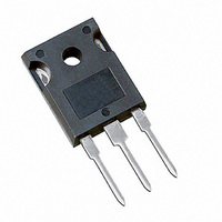
MOSFET N-CH 500V 31A TO-247AC
Manufacturer
Vishay
Specifications of IRFP31N50LPBF
Transistor Polarity
N-Channel
Fet Type
MOSFET N-Channel, Metal Oxide
Fet Feature
Standard
Rds On (max) @ Id, Vgs
180 mOhm @ 19A, 10V
Drain To Source Voltage (vdss)
500V
Current - Continuous Drain (id) @ 25° C
31A
Vgs(th) (max) @ Id
5V @ 250µA
Gate Charge (qg) @ Vgs
210nC @ 10V
Input Capacitance (ciss) @ Vds
5000pF @ 25V
Power - Max
460W
Mounting Type
Through Hole
Package / Case
TO-247-3 (Straight Leads), TO-247AC
Minimum Operating Temperature
- 55 C
Configuration
Single
Resistance Drain-source Rds (on)
0.18 Ohm @ 10 V
Drain-source Breakdown Voltage
500 V
Gate-source Breakdown Voltage
+/- 30 V
Continuous Drain Current
31 A
Power Dissipation
460000 mW
Maximum Operating Temperature
+ 150 C
Mounting Style
Through Hole
Continuous Drain Current Id
31A
Drain Source Voltage Vds
500V
On Resistance Rds(on)
180mohm
Rds(on) Test Voltage Vgs
10V
Threshold Voltage Vgs Typ
5V
Lead Free Status / RoHS Status
Lead free / RoHS Compliant
Lead Free Status / RoHS Status
Lead free / RoHS Compliant, Lead free / RoHS Compliant
Other names
*IRFP31N50LPBF
Available stocks
Company
Part Number
Manufacturer
Quantity
Price
Company:

Part Number:
IRFP31N50LPBF
Manufacturer:
TOREX
Quantity:
3 001
Company:
Part Number:
IRFP31N50LPBF
Manufacturer:
IR
Quantity:
4 250
Part Number:
IRFP31N50LPBF
Manufacturer:
IR
Quantity:
20 000


IRFP31N50L, SiHFP31N50L
Vishay Siliconix
www.vishay.com
4
THE PRODUCT DESCRIBED HEREIN AND THIS DATASHEET ARE SUBJECT TO SPECIFIC DISCLAIMERS, SET FORTH AT
1 000 000
100 000
10 000
Fig. 5 - Typical Capacitance vs. Drain-to-Source Voltage
1000
100
Fig. 6 - Output Capacitance Stored Energy vs. V
10
30
25
20
15
10
5
0
0
1
100
V DS , Drain-to-Source Voltage (V)
V DS , Drain-to-Source Voltage (V)
V GS = 0 V,
C iss = C gs + C gd , C ds
C rss = C gd
C oss = C ds + C gd
200
10
300
C oss
C rss
C iss
400
100
This datasheet is subject to change without notice.
SHORTED
f = 1 MHz
500
600
1000
DS
Fig. 7 - Typical Gate Charge vs. Gate-to-Source Voltage
1000
20
12
Fig. 8 - Typical Source Drain Diode Forward Voltage
100
0.1
10
8
4
0
1
0.2
0
I D = 31 A
T J = 150 °C
V SD , Source-to-Drain Voltage (V)
40
0.6
Q G , Total Gate Charge (nC)
T J = 25 °C
1.0
80
S11-0488-Rev. C, 21-Mar-11
www.vishay.com/doc?91000
Document Number: 91220
V DS = 400 V
V DS = 250 V
V DS = 100 V
120
1.4
V GS = 0 V
160
1.8
Related parts for IRFP31N50LPBF
Image
Part Number
Description
Manufacturer
Datasheet
Request
R

Part Number:
Description:
357-036-542-201 CARDEDGE 36POS DL .156 BLK LOPRO
Manufacturer:
Vishay
Datasheet:
Part Number:
Description:
357-036-542-201 CARDEDGE 36POS DL .156 BLK LOPRO
Manufacturer:
Vishay
Datasheet:
Part Number:
Description:
357-036-542-201 CARDEDGE 36POS DL .156 BLK LOPRO
Manufacturer:
Vishay
Datasheet:
Part Number:
Description:
357-036-542-201 CARDEDGE 36POS DL .156 BLK LOPRO
Manufacturer:
Vishay
Datasheet:
Part Number:
Description:
357-036-542-201 CARDEDGE 36POS DL .156 BLK LOPRO
Manufacturer:
Vishay
Datasheet:
Part Number:
Description:
357-036-542-201 CARDEDGE 36POS DL .156 BLK LOPRO
Manufacturer:
Vishay
Datasheet:
Part Number:
Description:
357-036-542-201 CARDEDGE 36POS DL .156 BLK LOPRO
Manufacturer:
Vishay
Datasheet:
Part Number:
Description:
357-036-542-201 CARDEDGE 36POS DL .156 BLK LOPRO
Manufacturer:
Vishay
Datasheet:
Part Number:
Description:
357-036-542-201 CARDEDGE 36POS DL .156 BLK LOPRO
Manufacturer:
Vishay
Datasheet:
Part Number:
Description:
357-036-542-201 CARDEDGE 36POS DL .156 BLK LOPRO
Manufacturer:
Vishay
Datasheet:
Part Number:
Description:
357-036-542-201 CARDEDGE 36POS DL .156 BLK LOPRO
Manufacturer:
Vishay
Datasheet:
Part Number:
Description:
357-036-542-201 CARDEDGE 36POS DL .156 BLK LOPRO
Manufacturer:
Vishay
Datasheet:
Part Number:
Description:
357-036-542-201 CARDEDGE 36POS DL .156 BLK LOPRO
Manufacturer:
Vishay
Datasheet:
Part Number:
Description:
357-036-542-201 CARDEDGE 36POS DL .156 BLK LOPRO
Manufacturer:
Vishay
Datasheet:
Part Number:
Description:
357-036-542-201 CARDEDGE 36POS DL .156 BLK LOPRO
Manufacturer:
Vishay
Datasheet: