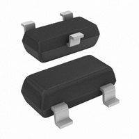
PMV213SN,215 NXP Semiconductors, PMV213SN,215 Datasheet - Page 5

PMV213SN,215
Manufacturer Part Number
PMV213SN,215
Description
MOSFET N-CH 100V 1.9A SOT23
Manufacturer
NXP Semiconductors
Series
TrenchMOS™r
Datasheet
1.PMV213SN215.pdf
(12 pages)
Specifications of PMV213SN,215
Package / Case
SOT-23-3, TO-236-3, Micro3™, SSD3, SST3
Fet Type
MOSFET N-Channel, Metal Oxide
Fet Feature
Logic Level Gate
Rds On (max) @ Id, Vgs
250 mOhm @ 500mA, 10V
Drain To Source Voltage (vdss)
100V
Current - Continuous Drain (id) @ 25° C
1.9A
Vgs(th) (max) @ Id
4V @ 1mA
Gate Charge (qg) @ Vgs
7nC @ 10V
Input Capacitance (ciss) @ Vds
330pF @ 20V
Power - Max
2W
Mounting Type
Surface Mount
Minimum Operating Temperature
- 55 C
Configuration
Single
Transistor Polarity
N-Channel
Resistance Drain-source Rds (on)
0.25 Ohm @ 10 V
Drain-source Breakdown Voltage
100 V
Gate-source Breakdown Voltage
+/- 30 V
Continuous Drain Current
1.9 A
Power Dissipation
2000 mW
Maximum Operating Temperature
+ 150 C
Mounting Style
SMD/SMT
Lead Free Status / RoHS Status
Lead free / RoHS Compliant
Lead Free Status / RoHS Status
Lead free / RoHS Compliant, Lead free / RoHS Compliant
Other names
934057521215
PMV213SN T/R
PMV213SN T/R
PMV213SN T/R
PMV213SN T/R
Available stocks
Company
Part Number
Manufacturer
Quantity
Price
Company:
Part Number:
PMV213SN,215
Manufacturer:
HEXAWAVE
Quantity:
3 680
Part Number:
PMV213SN,215
Manufacturer:
NEXPERIA/安世
Quantity:
20 000
Philips Semiconductors
5. Characteristics
Table 4:
T
9397 750 11128
Product data
Symbol Parameter
Static characteristics
V
V
I
I
R
Dynamic characteristics
Q
Q
Q
C
C
C
t
t
t
t
Source-drain diode
V
t
Q
DSS
GSS
d(on)
r
d(off)
f
rr
j
(BR)DSS
GS(th)
SD
DSon
iss
oss
rss
g(tot)
gs
gd
r
= 25 C unless otherwise specified.
drain-source breakdown voltage
gate-source threshold voltage
drain-source leakage current
gate-source leakage current
drain-source on-state resistance
total gate charge
gate-source charge
gate-drain (Miller) charge
input capacitance
output capacitance
reverse transfer capacitance
turn-on delay time
rise time
turn-off delay time
fall time
source-drain (diode forward) voltage I
reverse recovery time
recovered charge
Characteristics
Conditions
I
I
V
V
V
I
V
V
I
D
D
D
S
S
Rev. 02 — 19 February 2003
DS
GS
GS
GS
DD
T
T
T
T
T
T
T
T
T
= 1.5 A; V
= 1.2 A; dI
= 250 A; V
= 1 mA; V
= 1.2 A; V
j
j
j
j
j
j
j
j
j
= 100 V; V
= 20 V; V
= 10 V; I
= 0 V; V
= 50 V; R
= 25 C
= 55 C
= 25 C
= 150 C
= 55 C
= 25 C
= 150 C
= 25 C
= 150 C
GS
DS
DD
DS
S
D
L
/dt = 100 A/ s; V
GS
= 0.5 A;
GS
DS
= V
= 80 V; V
= 20 V; f = 1 MHz;
= 33 ; V
= 0 V;
= 0 V
= 0 V
= 0 V
GS
;
Figure 12
Figure 9
Figure 7
GS
GS
= 10 V;
= 10 V; R
GS
and
Figure 11
= 0 V
Figure 13
8
TrenchMOS™ standard level FET
G
= 6
© Koninklijke Philips Electronics N.V. 2003. All rights reserved.
PMV213SN
Min
100
90
2
1.2
-
-
-
-
-
-
-
-
-
-
-
-
-
-
-
-
-
-
-
Typ
-
-
3
-
-
-
-
10
213
490
7
1.4
2.5
330
36
22
5.5
5
9.5
3
0.83
36
23
Max
-
-
4
-
4.4
1
100
100
250
575
-
-
-
-
-
-
-
-
-
-
1.2
-
-
5 of 12
Unit
V
V
V
V
V
nA
m
m
nC
nC
nC
pF
pF
pF
ns
ns
ns
ns
V
ns
nC
A
A


