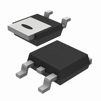
PSMN063-150D,118 NXP Semiconductors, PSMN063-150D,118 Datasheet

PSMN063-150D,118
Specifications of PSMN063-150D,118
PSMN063-150D /T3
PSMN063-150D /T3
Related parts for PSMN063-150D,118
PSMN063-150D,118 Summary of contents
Page 1
... N-channel enhancement mode field-effect transistor Rev. 03 — 31 October 2001 1. Product profile 1.1 Description N-channel enhancement mode field-effect transistor in a plastic package using TrenchMOS Product availability: PSMN063-150D in SOT428 (D-PAK). 1.2 Features TrenchMOS™ technology Fast Switching 1.3 Applications converters 1.4 Quick reference data ...
Page 2
... C; pulsed Figure Figure pulsed unclamped inductive load 0.2 ms starting unclamped inductive load starting Rev. 03 — 31 October 2001 PSMN063-150D Min Max Unit 150 V 150 116 A 150 W 55 +175 C 55 +175 116 A 502 © Koninklijke Philips Electronics N.V. 2001. All rights reserved ...
Page 3
... N-channel enhancement mode field-effect transistor 03aa16 120 I der (%) 150 200 der Fig 2. Normalized continuous drain current as a function of mounting base temperature Rev. 03 — 31 October 2001 PSMN063-150D 03aa24 50 100 150 ------------------- 100 003aaa148 100 100 (V) © Koninklijke Philips Electronics N.V. 2001. All rights reserved. 200 ...
Page 4
... Fig 4. Transient thermal impedance from junction to mounting base as a function of pulse duration. 9397 750 08594 Product data N-channel enhancement mode field-effect transistor Conditions Figure 4 Vertical in still air Rev. 03 — 31 October 2001 PSMN063-150D Value Unit 1.0 K/W 50 K/W 003aaa149 (s) © ...
Page 5
... Figure 175 150 175 Figure 7 and 175 120 Figure MHz; Figure 2 5 Figure /dt = 100 Rev. 03 — 31 October 2001 PSMN063-150D Typ Max Unit 0. 500 A 0.02 100 176 2390 pF 240 0.9 1.2 V 105 ns 0.55 C © Koninklijke Philips Electronics N.V. 2001. All rights reserved ...
Page 6
... C and 175 Fig 6. Transfer characteristics: drain current as a function of gate-source voltage; typical values. 003aaa151 2.8 a 2.4 2.0 1.6 6 1 (A) Fig 8. Normalized drain source on-state resistance factor as a function of junction temperature. Rev. 03 — 31 October 2001 PSMN063-150D 003aaa152 175 ( DSon 03aa30 140 - 100 - ...
Page 7
... Fig 10. Sub-threshold drain current as a function of gate-source voltage. 003aaa153 (pF ( MHz GS Fig 12. Input, output and reverse transfer capacitances as a function of drain-source voltage; typical values. Rev. 03 — 31 October 2001 PSMN063-150D 03aa35 typ min max ( 003aaa154 C iss C oss C rss (V) © Koninklijke Philips Electronics N.V. 2001. All rights reserved. 6 ...
Page 8
... Product data N-channel enhancement mode field-effect transistor 003aaa156 ( 1 ( Fig 14. Gate-source voltage as a function of gate charge; typical values. Rev. 03 — 31 October 2001 PSMN063-150D 003aaa155 120 (nC and 120 V DD © Koninklijke Philips Electronics N.V. 2001. All rights reserved ...
Page 9
... REFERENCES JEDEC EIAJ TO-252 SC-63 Rev. 03 — 31 October 2001 PSMN063-150D max. min. 10.4 2.95 0.7 0.5 0.2 9.6 2.55 0.5 EUROPEAN ISSUE DATE PROJECTION ...
Page 10
... Philips Semiconductors 7. Revision history Table 5: Revision history Rev Date CPCN Description 03 20011031 - Product data; third version; supersedes second version PSMN063_150D_2 of 1 August 1999. • Max value 19990801 - Product specification; second version PSMN063_150D_2; supersedes initial Lotus Manuscript version of August 1999 Rev 1.000. 01 ...
Page 11
... Rev. 03 — 31 October 2001 Rev. 03 — 31 October 2001 PSMN063-150D PSMN063-150D Fax: + 24825 © Koninklijke Philips Electronics N.V. 2001. All rights reserved. © Koninklijke Philips Electronics N.V. 2001. All rights reserved ...
Page 12
... Publication thereof does not convey nor imply any license under patent- or other industrial or intellectual property rights. Date of release: 31 October 2001 Document order number: 9397 750 08594 PSMN063-150D N-channel enhancement mode field-effect transistor ...


