IRFZ44N,127 NXP Semiconductors, IRFZ44N,127 Datasheet - Page 2
IRFZ44N,127
Manufacturer Part Number
IRFZ44N,127
Description
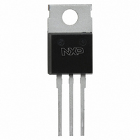
MOSFET N-CH 55V 49A SOT78
Manufacturer
NXP Semiconductors
Series
TrenchMOS™r
Datasheet
1.IRFZ44N127.pdf
(8 pages)
Specifications of IRFZ44N,127
Fet Type
MOSFET N-Channel, Metal Oxide
Fet Feature
Standard
Rds On (max) @ Id, Vgs
22 mOhm @ 25A, 10V
Drain To Source Voltage (vdss)
55V
Current - Continuous Drain (id) @ 25° C
49A
Vgs(th) (max) @ Id
4V @ 1mA
Gate Charge (qg) @ Vgs
62nC @ 10V
Input Capacitance (ciss) @ Vds
1800pF @ 25V
Power - Max
110W
Mounting Type
Through Hole
Package / Case
TO-220AB-3
Lead Free Status / RoHS Status
Lead free / RoHS Compliant
Other names
934055538127
IRFZ44NP
IRFZ44NP
IRFZ44NP
IRFZ44NP


Philips Semiconductors
STATIC CHARACTERISTICS
T
DYNAMIC CHARACTERISTICS
T
REVERSE DIODE LIMITING VALUES AND CHARACTERISTICS
T
February 1999
N-channel enhancement mode
TrenchMOS
j
SYMBOL PARAMETER
V
V
I
I
R
mb
SYMBOL PARAMETER
g
C
C
C
Q
Q
Q
t
t
t
t
L
L
L
j
SYMBOL PARAMETER
I
I
V
t
Q
= 25˚C unless otherwise specified
DSS
GSS
d on
r
d off
f
DR
DRM
rr
= 25˚C unless otherwise specified
V
fs
d
d
s
(BR)DSS
GS(TO)
SD
DS(ON)
iss
oss
rss
g
gs
gd
rr
= 25˚C unless otherwise specified
(BR)GSS
Drain-source breakdown
voltage
Gate threshold voltage
Zero gate voltage drain current
Gate source leakage current
Gate source breakdown voltage I
Drain-source on-state
resistance
Forward transconductance
Input capacitance
Output capacitance
Feedback capacitance
Total gate charge
Gate-cource charge
Gate-drain (miller) charge
Turn-on delay time
Turn-on rise time
Turn-off delay time
Turn-off fall time
Internal drain inductance
Internal drain inductance
Internal source inductance
Continuous reverse drain
current
Pulsed reverse drain current
Diode forward voltage
Reverse recovery time
Reverse recovery charge
TM
transistor
CONDITIONS
V
V
V
V
V
CONDITIONS
V
V
V
V
V
Resistive load
Measured from contact screw on
tab to centre of die
Measured from drain lead 6 mm
from package to centre of die
Measured from source lead 6 mm
from package to source bond pad
CONDITIONS
I
I
I
V
G
F
F
F
GS
DS
DS
GS
GS
DS
GS
DD
DD
GS
GS
= 25 A; V
= 40 A; V
= 40 A; -dI
= 1 mA;
= 0 V; I
= V
= 55 V; V
= 10 V; V
= 10 V; I
= 25 V; I
= 0 V; V
= 44 V; I
= 30 V; I
= 10 V; R
= -10 V; V
GS
; I
2
D
D
GS
GS
DS
D
D
D
D
F
= 0.25 mA;
= 1 mA
GS
/dt = 100 A/ s;
G
= 25 A
= 25 A
= 50 A; V
= 25 A;
= 0 V
= 0 V
R
DS
= 25 V; f = 1 MHz
= 10
= 30 V
= 0 V;
= 0 V
GS
T
T
T
T
T
T
j
j
j
j
j
j
= 10 V
= 175˚C
= 175˚C
= 175˚C
= 175˚C
= -55˚C
= -55˚C
MIN.
MIN.
MIN.
2.0
1.0
55
50
16
6
-
-
-
-
-
-
-
-
-
-
-
-
-
-
-
-
-
-
-
-
-
-
-
-
-
-
TYP.
TYP.
1350
TYP.
0.05
0.04
0.95
0.15
330
155
3.0
3.5
4.5
7.5
1.0
15
18
50
40
30
47
-
-
-
-
-
-
-
-
-
-
-
-
-
-
Product specification
MAX.
MAX.
MAX.
1800
500
400
215
160
4.0
4.4
1.2
10
20
22
42
62
15
26
26
75
50
40
49
IRFZ44N
1
-
-
-
-
-
-
-
-
-
-
-
Rev 1.000
UNIT
UNIT
UNIT
m
m
nC
nC
nC
nH
nH
nH
pF
pF
pF
ns
ns
ns
ns
ns
V
V
V
V
V
S
A
A
V
C
A
A
A
A
Related parts for IRFZ44N,127
Image
Part Number
Description
Manufacturer
Datasheet
Request
R

Part Number:
Description:
NXP Semiconductors designed the LPC2420/2460 microcontroller around a 16-bit/32-bitARM7TDMI-S CPU core with real-time debug interfaces that include both JTAG andembedded trace
Manufacturer:
NXP Semiconductors
Datasheet:

Part Number:
Description:
NXP Semiconductors designed the LPC2458 microcontroller around a 16-bit/32-bitARM7TDMI-S CPU core with real-time debug interfaces that include both JTAG andembedded trace
Manufacturer:
NXP Semiconductors
Datasheet:
Part Number:
Description:
NXP Semiconductors designed the LPC2468 microcontroller around a 16-bit/32-bitARM7TDMI-S CPU core with real-time debug interfaces that include both JTAG andembedded trace
Manufacturer:
NXP Semiconductors
Datasheet:
Part Number:
Description:
NXP Semiconductors designed the LPC2470 microcontroller, powered by theARM7TDMI-S core, to be a highly integrated microcontroller for a wide range ofapplications that require advanced communications and high quality graphic displays
Manufacturer:
NXP Semiconductors
Datasheet:
Part Number:
Description:
NXP Semiconductors designed the LPC2478 microcontroller, powered by theARM7TDMI-S core, to be a highly integrated microcontroller for a wide range ofapplications that require advanced communications and high quality graphic displays
Manufacturer:
NXP Semiconductors
Datasheet:
Part Number:
Description:
The Philips Semiconductors XA (eXtended Architecture) family of 16-bit single-chip microcontrollers is powerful enough to easily handle the requirements of high performance embedded applications, yet inexpensive enough to compete in the market for hi
Manufacturer:
NXP Semiconductors
Datasheet:
Part Number:
Description:
The XA-S3 device is a member of Philips Semiconductors? XA(eXtended Architecture) family of high performance 16-bitsingle-chip microcontrollers
Manufacturer:
NXP Semiconductors
Datasheet:

Part Number:
Description:
The NXP BlueStreak LH75401/LH75411 family consists of two low-cost 16/32-bit System-on-Chip (SoC) devices
Manufacturer:
NXP Semiconductors
Datasheet:
Part Number:
Description:
The NXP LPC3130/3131 combine an 180 MHz ARM926EJ-S CPU core, high-speed USB2
Manufacturer:
NXP Semiconductors
Datasheet:
Part Number:
Description:
The NXP LPC3141 combine a 270 MHz ARM926EJ-S CPU core, High-speed USB 2
Manufacturer:
NXP Semiconductors
Part Number:
Description:
The NXP LPC3143 combine a 270 MHz ARM926EJ-S CPU core, High-speed USB 2
Manufacturer:
NXP Semiconductors

Part Number:
Description:
The NXP LPC3152 combines an 180 MHz ARM926EJ-S CPU core, High-speed USB 2
Manufacturer:
NXP Semiconductors
Part Number:
Description:
The NXP LPC3154 combines an 180 MHz ARM926EJ-S CPU core, High-speed USB 2
Manufacturer:
NXP Semiconductors

Part Number:
Description:
Standard level N-channel enhancement mode Field-Effect Transistor (FET) in a plastic package using NXP High-Performance Automotive (HPA) TrenchMOS technology
Manufacturer:
NXP Semiconductors
Datasheet: