APT18F60B Microsemi Power Products Group, APT18F60B Datasheet - Page 4
APT18F60B
Manufacturer Part Number
APT18F60B
Description
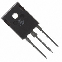
MOSFET N-CH 600V 18A TO-247
Manufacturer
Microsemi Power Products Group
Datasheet
1.APT18F60B.pdf
(4 pages)
Specifications of APT18F60B
Fet Type
MOSFET N-Channel, Metal Oxide
Fet Feature
Standard
Rds On (max) @ Id, Vgs
390 mOhm @ 9A, 10V
Drain To Source Voltage (vdss)
600V
Current - Continuous Drain (id) @ 25° C
18A
Vgs(th) (max) @ Id
5V @ 1mA
Gate Charge (qg) @ Vgs
90nC @ 10V
Input Capacitance (ciss) @ Vds
3550pF @ 25V
Power - Max
335W
Mounting Type
Through Hole
Package / Case
TO-247
Lead Free Status / RoHS Status
Lead free / RoHS Compliant
Other names
APT18F60BMI
APT18F60BMI
APT18F60BMI
Available stocks
Company
Part Number
Manufacturer
Quantity
Price
Company:

Part Number:
APT18F60B
Manufacturer:
Microsemi Power Products Group
Quantity:
135


Microsemi’s products are covered by one or more of U.S. patents 4,895,810 5,045,903 5,089,434 5,182,234 5,019,522 5,262,336 6,503,786 5,256,583
4,748,103 5,283,202 5,231,474 5,434,095 5,528,058 6,939,743, 7,352,045 5,283,201 5,801,417 5,648,283 7,196,634 6,664,594 7,157,886 6,939,743 7,342,262
and foreign patents. US and Foreign patents pending. All Rights Reserved.
0.40 (.016)
0.79 (.031)
2.21 (.087)
2.59 (.102)
0.40
0.35
0.30
0.25
0.20
0.15
0.10
0.05
4.69 (.185)
5.31 (.209)
1.49 (.059)
2.49 (.098)
100
0.1
10
1
0
10
1
Dimensions in Millimeters and (Inches)
T
-5
T
Figure 9, Forward Safe Operating Area
J
V
C
=
DS
=
I
R ds(on)
DM
125°C
20.80 (.819)
21.46 (.845)
19.81 (.780)
20.32 (.800)
75°C
, DRAIN-TO-SOURCE VOLTAGE (V)
D = 0.9
TO-247 (B) Package Outline
0.7
0.3
0.1
0.5
0.05
6.15 (.242) BSC
4.50 (.177) Max.
Figure 11. Maximum Effective Transient Thermal Impedance Junction-to-Case vs Pulse Duration
1.01 (.040)
1.40 (.055)
10
5.45 (.215) BSC
13µs
2-Plcs.
100µs
1ms
100ms
10ms
DC line
10
15.49 (.610)
16.26 (.640)
-4
100
5.38 (.212)
6.20 (.244)
3.50 (.138)
3.81 (.150)
2.87 (.113)
3.12 (.123)
1.65 (.065)
2.13 (.084)
Gate
Drain
Source
RECTANGULAR PULSE DURATION (seconds)
800
10
SINGLE PULSE
-3
e3 100% Sn Plated
4.98 (.196)
5.08 (.200)
1.47 (.058)
1.57 (.062)
0.46 (.018)
0.56 (.022)
0.020 (.001)
0.178 (.007)
2.67 (.105)
2.84 (.112)
10
100
0.1
10
Figure 10, Maximum Forward Safe Operating Area
-2
1
1
Scaling for Different Case & Junction
Temperatures:
{3 Plcs}
R ds(on)
T
T
V
J
C
I
1.22 (.048)
1.32 (.052)
D
DS
=
=
I
=
DM
150°C
D
, DRAIN-TO-SOURCE VOLTAGE (V)
25°C
I
D(T
Dimensions in Millimeters (Inches)
3
PAK Package Outline
C
= 25
10
Note:
15.95 (.628)
16.05(.632)
°
C)
Revised
Peak T J = P DM x Z θJC + T C
4/18/95
13µs
100µs
*(
Duty Factor D =
10
T
1ms
t
J
1
-1
10ms
-
100ms
= Pulse Duration
1.98 (.078)
2.08 (.082)
5.45 (.215) BSC
{2 Plcs.}
T
DC line
t 1
Gate
C
)/125
13.79 (.543)
13.99(.551)
Drain
t 2
100
Source
1.04 (.041)
1.15(.045)
1.27 (.050)
1.40 (.055)
t 1
/
t 2
APT18F60B_S
13.41 (.528)
13.51(.532)
1.0
800
Revised
8/29/97
Heat Sink (Drain)
and Leads
are Plated
3.81 (.150)
4.06 (.160)
(Base of Lead)
11.51 (.453)
11.61 (.457)
Related parts for APT18F60B
Image
Part Number
Description
Manufacturer
Datasheet
Request
R

Part Number:
Description:
IGBT 600V 100A 463W TO247
Manufacturer:
Microsemi Power Products Group
Datasheet:

Part Number:
Description:
IGBT 600V 198A 833W TO264
Manufacturer:
Microsemi Power Products Group
Datasheet:
Part Number:
Description:
IGBT 600V 41A 187W TO247
Manufacturer:
Microsemi Power Products Group
Datasheet:
Part Number:
Description:
MOSFET N-CH 600V 23A TO-247
Manufacturer:
Microsemi Power Products Group
Datasheet:

Part Number:
Description:
MOSFET N-CH 500V 17A TO-220
Manufacturer:
Microsemi Power Products Group
Datasheet:
Part Number:
Description:
MOSFET N-CH 1200V 3.5A TO-220
Manufacturer:
Microsemi Power Products Group
Datasheet:
Part Number:
Description:
MOSFET N-CH 500V 22A TO-247
Manufacturer:
Microsemi Power Products Group
Datasheet:
Part Number:
Description:
MOSFET N-CH 100V 75A TO-247
Manufacturer:
Microsemi Power Products Group
Datasheet:
Part Number:
Description:
MOSFET N-CH 200V 56A TO-247
Manufacturer:
Microsemi Power Products Group
Datasheet:
Part Number:
Description:
MOSFET N-CH 500V 27A TO-247
Manufacturer:
Microsemi Power Products Group
Datasheet:
Part Number:
Description:
MOSFET N-CH 300V 40A TO-247
Manufacturer:
Microsemi Power Products Group
Datasheet:
Part Number:
Description:
MOSFET N-CH 200V 59A TO-247
Manufacturer:
Microsemi Power Products Group
Datasheet:
Part Number:
Description:
MOSFET N-CH 500V 26A TO-247
Manufacturer:
Microsemi Power Products Group
Datasheet:
Part Number:
Description:
MOSFET N-CH 300V 40A TO-247
Manufacturer:
Microsemi Power Products Group
Datasheet:
Part Number:
Description:
MOSFET N-CH 200V 65A TO-247
Manufacturer:
Microsemi Power Products Group
Datasheet: