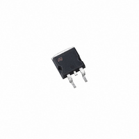
STB100NF04T4 STMicroelectronics, STB100NF04T4 Datasheet

STB100NF04T4
Specifications of STB100NF04T4
Available stocks
Related parts for STB100NF04T4
STB100NF04T4 Summary of contents
Page 1
... Standard threshold drive ■ 100% avalanche tested Description This Power MOSFET is the latest development of STMicroelectronics unique “Single Feature Size™” strip-based process. The resulting transistor shows extremely high packing density for low on-resistance, rugged avalanche characteristics and less critical alignment steps therefore a remarkable manufacturing reproducibility ...
Page 2
Contents: Contents: 1 Electrical ratings . . . . . . . . . . . . . . . . . . . . . . . . . . . . . . . . . . . ...
Page 3
STB100NF04 - STP100NF04 1 Electrical ratings Table 1. Absolute maximum ratings Symbol Drain-source Voltage ( Gate-source Voltage GS (1) I Drain-current (continuous) at Tc=25°C D (1) I Drain-current (continuous) at Tc=100°C D (2) I Drain-current (pulsed) DM ...
Page 4
Electrical characteristics 2 Electrical characteristics (T =25°C unless otherwise specified) CASE Table 3. On/off Symbol Drain-source Breakdown V (BR)DSS Voltage Zero Gate Voltage Drain I DSS Current (V Gate-body Leakage I GSS Current (V V Gate Threshold Voltage GS(th) Static ...
Page 5
STB100NF04 - STP100NF04 Table 5. Source drain diode Symbol I Source-drain Current SD (1) I Source-drain Current (pulsed) SDM (2) V Forward on Voltage SD t Reverse Recovery Time rr Q Reverse Recovery Charge rr I Reverse recovery Current RRM ...
Page 6
Electrical characteristics 2.1 Electrical characteristics (curves) Figure 1. Power Derating vs. Tc Figure 3. Output Characteristics Figure 5. Transconductance 6/17 STB100NF04 - STP100NF04 Figure 2. Max Id Current vs. Tc Figure 4. Transfer Characteristics Figure 6. Static Drain-source on Resistance ...
Page 7
STB100NF04 - STP100NF04 Figure 7. Gate Charge vs. Gate-source Voltage Figure 9. Normalized Gate Threshold Voltage vs. Temperature Figure 11. Source-Drain Diode Forward Characteristics Electrical characteristics Figure 8. Capacitance Variations Figure 10. Normalized on Resistance vs. Temperature Figure 12. Normalized ...
Page 8
Electrical characteristics Figure 13. Thermal Resistance Rthj-pcb vs. PCB Copper Area Figure 15. Max Power Dissipation vs. PCB Copper Area 8/17 STB100NF04 - STP100NF04 Figure 14. Thermal Impedance Figure 16. Safe Operating Area ...
Page 9
STB100NF04 - STP100NF04 Figure 17. Allowable Iav vs. Time in Avalanche The previous curve give the safe operating area for unclamped inductive loads, single pulse or repetitive, under the following conditions 0.5*(1.3*BV D(AVE AS(AR) D(AVE) ...
Page 10
Electrical characteristics 2.2 Spice thermal model Table 6. Spice parameter Parameter CTHERM1 CTHERM1 CTHERM3 CTHERM4 RTHERM1 RTHERM2 RTHERM3 RTHERM4 Figure 18. Spice model schematic 10/17 STB100NF04 - STP100NF04 Node ...
Page 11
STB100NF04 - STP100NF04 3 Test circuit Figure 19. Unclamped inductive load test circuit Figure 21. Switching times test circuit for resistive load Figure 23. Test circuit for inductive load switching Figure 20. Unclamped inductive waveform Figure 22. Gate charge test ...
Page 12
Package mechanical data 4 Package mechanical data In order to meet environmental requirements, ST offers these devices in ECOPACK® packages. These packages have a Lead-free second level interconnect. The category of second level interconnect is marked on the package and ...
Page 13
STB100NF04 - STP100NF04 DIM L20 L30 øP Q TO-220 MECHANICAL DATA mm. MIN. TYP MAX. 4.40 4.60 0.61 0.88 1.15 1.70 0.49 0.70 15.25 15.75 10 10.40 ...
Page 14
Package mechanical data DIM 14/ PAK MECHANICAL DATA TO-247 MECHANICAL DATA mm. MIN. TYP MAX. 4.4 4.6 2.49 2.69 0.03 ...
Page 15
STB100NF04 - STP100NF04 5 Packaging mechanical data 2 D PAK FOOTPRINT TAPE MECHANICAL DATA mm DIM. MIN. MAX. A0 10.5 10.7 B0 15.7 15.9 D 1.5 1.6 D1 1.59 1.61 E 1.65 1.85 F 11.4 11.6 K0 4.8 5.0 P0 ...
Page 16
Revision history 6 Revision history Table 7. Revision history Date 23-Mar-2005 01-Mar-2006 04-Sep-2006 20-Feb-2007 16/17 Revision 2 New template 3 Removed I²PAK and inserted D²PAK. 4 New template, no content change 5 Typo mistake on page 1 STB100NF04 - STP100NF04 ...
Page 17
... STB100NF04 - STP100NF04 Information in this document is provided solely in connection with ST products. STMicroelectronics NV and its subsidiaries (“ST”) reserve the right to make changes, corrections, modifications or improvements, to this document, and the products and services described herein at any time, without notice. All ST products are sold pursuant to ST’s terms and conditions of sale. ...


