IRF540NPBF International Rectifier, IRF540NPBF Datasheet - Page 2
IRF540NPBF
Manufacturer Part Number
IRF540NPBF
Description
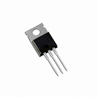
MOSFET N-CH 100V 33A TO-220AB
Manufacturer
International Rectifier
Series
HEXFET®r
Specifications of IRF540NPBF
Fet Type
MOSFET N-Channel, Metal Oxide
Fet Feature
Standard
Rds On (max) @ Id, Vgs
44 mOhm @ 16A, 10V
Drain To Source Voltage (vdss)
100V
Current - Continuous Drain (id) @ 25° C
33A
Vgs(th) (max) @ Id
4V @ 250µA
Gate Charge (qg) @ Vgs
71nC @ 10V
Input Capacitance (ciss) @ Vds
1960pF @ 25V
Power - Max
130W
Mounting Type
Through Hole
Package / Case
TO-220-3 (Straight Leads)
Current, Drain
33 A
Gate Charge, Total
71 nC
Package Type
TO-220AB
Polarization
N-Channel
Power Dissipation
130 W
Resistance, Drain To Source On
44 Milliohms
Temperature, Operating, Maximum
+175 °C
Temperature, Operating, Minimum
-55 °C
Time, Turn-off Delay
39 ns
Time, Turn-on Delay
11 ns
Transconductance, Forward
21 S
Voltage, Breakdown, Drain To Source
100 V
Voltage, Forward, Diode
1.2 V
Voltage, Gate To Source
±20 V
Transistor Polarity
N-Channel
Drain-source Breakdown Voltage
100 V
Gate-source Breakdown Voltage
20 V
Continuous Drain Current
33 A
Mounting Style
Through Hole
Gate Charge Qg
47.3 nC
Lead Free Status / RoHS Status
Lead free / RoHS Compliant
Other names
*IRF540NPBF
Available stocks
Company
Part Number
Manufacturer
Quantity
Price
Company:

Part Number:
IRF540NPBF
Manufacturer:
IR
Quantity:
13 000
Part Number:
IRF540NPBF
Manufacturer:
IR
Quantity:
20 000


Source-Drain Ratings and Characteristics
IRF540NPbF
Electrical Characteristics @ T
Notes:
I
I
V
∆V
R
V
g
Q
Q
Q
t
t
t
t
C
C
C
E
I
I
V
t
Q
t
L
L
DSS
GSS
SM
d(on)
d(off)
S
rr
on
r
f
2
fs
D
S
(BR)DSS
GS(th)
AS
SD
DS(on)
iss
oss
rss
rr
g
gs
gd
Repetitive rating; pulse width limited by
(BR)DSS
max. junction temperature. (See fig. 11)
R
Starting T
G
= 25Ω, I
/∆T
J
J
Drain-to-Source Leakage Current
Drain-to-Source Breakdown Voltage
Breakdown Voltage Temp. Coefficient
Static Drain-to-Source On-Resistance
Gate Threshold Voltage
Forward Transconductance
Gate-to-Source Forward Leakage
Gate-to-Source Reverse Leakage
Total Gate Charge
Gate-to-Source Charge
Gate-to-Drain ("Miller") Charge
Turn-On Delay Time
Rise Time
Turn-Off Delay Time
Fall Time
Input Capacitance
Output Capacitance
Reverse Transfer Capacitance
Single Pulse Avalanche Energy
Continuous Source Current
(Body Diode)
Pulsed Source Current
(Body Diode)
Diode Forward Voltage
Reverse Recovery Time
Reverse Recovery Charge
Forward Turn-On Time
Internal Drain Inductance
Internal Source Inductance
= 25°C, L =1.5mH
AS
= 16A. (See Figure 12)
Parameter
Parameter
J
= 25°C (unless otherwise specified)
I
Pulse width ≤ 400µs; duty cycle ≤ 2%.
This is a typical value at device destruction and represents
T
This is a calculated value limited to T
operation outside rated limits.
SD
100
–––
–––
–––
–––
–––
–––
–––
–––
–––
–––
–––
–––
–––
–––
–––
–––
–––
––– 700
Min. Typ. Max. Units
Min. Typ. Max. Units
2.0
–––
–––
–––
–––
–––
21
–––
J
≤ 175°C
Intrinsic turn-on time is negligible (turn-on is dominated by L
≤ 16A, di/dt ≤ 340A/µs, V
1960 –––
0.12
505
–––
–––
–––
–––
–––
–––
–––
––– -100
–––
–––
–––
250
–––
–––
–––
115
4.5
11
35
39
35
40
7.5
185
–––
170
760
–––
–––
–––
250
100
–––
–––
–––
–––
–––
–––
–––
1.2
4.0
44
25
71
14
110
21
33
V/°C Reference to 25°C, I
mΩ
mJ
nC
µA
nA
nC
ns
nH
pF
ns
V
V
S
A
V
ƒ = 1.0MHz, See Fig. 5
MOSFET symbol
showing the
integral reverse
p-n junction diode.
T
T
di/dt = 100A/µs
V
V
V
V
V
V
V
V
I
V
V
V
I
R
V
Between lead,
6mm (0.25in.)
from package
and center of die contact
V
V
I
DD
D
D
AS
GS
GS
DS
DS
DS
DS
GS
GS
DS
GS
DD
GS
GS
DS
J
J
G
= 16A
= 16A
= 25°C, I
= 25°C, I
≤ V
= 16A, L = 1.5mH
= 5.1Ω
= V
= 50V, I
= 100V, V
= 80V, V
= 80V
= 25V
= 0V, I
= 10V, I
= 20V
= -20V
= 10V, See Fig. 6 and 13
= 50V
= 10V, See Fig. 10
= 0V
(BR)DSS
GS
J
, I
= 175°C .
D
S
F
D
D
D
Conditions
= 250µA
GS
Conditions
= 16A
= 16A, V
,
= 250µA
= 16A
= 16A
GS
= 0V, T
= 0V
www.irf.com
D
GS
= 1mA
J
= 150°C
= 0V
G
G
S
+L
D
S
D
)
S
D
Related parts for IRF540NPBF
Image
Part Number
Description
Manufacturer
Datasheet
Request
R

Part Number:
Description:
SCHOTTKY RECTIFIER
Manufacturer:
International Rectifier Corp.
Datasheet:
Part Number:
Description:
SCHOTTKY RECTIFIER
Manufacturer:
International Rectifier Corp.
Datasheet:
Part Number:
Description:
SCHOTTKY RECTIFIER
Manufacturer:
International Rectifier Corp.
Datasheet:
Part Number:
Description:
SCHOTTKY RECTIFIER
Manufacturer:
International Rectifier Corp.
Datasheet:
Part Number:
Description:
SCHOTTKY RECTIFIER
Manufacturer:
International Rectifier Corp.
Datasheet:
Part Number:
Description:
SCHOTTKY RECTIFIER
Manufacturer:
International Rectifier Corp.
Datasheet:
Part Number:
Description:
SCHOTTKY RECTIFIER
Manufacturer:
International Rectifier Corp.
Datasheet:
Part Number:
Description:
SCHOTTKY RECTIFIER
Manufacturer:
International Rectifier Corp.
Datasheet:
Part Number:
Description:
SCHOTTKY RECTIFIER
Manufacturer:
International Rectifier Corp.
Datasheet:
Part Number:
Description:
SCHOTTKY RECTIFIER
Manufacturer:
International Rectifier Corp.
Datasheet:
Part Number:
Description:
SCHOTTKY RECTIFIER
Manufacturer:
International Rectifier Corp.
Datasheet:
Part Number:
Description:
SCHOTTKY RECTIFIER
Manufacturer:
International Rectifier Corp.
Datasheet:
Part Number:
Description:
SCHOTTKY RECTIFIER
Manufacturer:
International Rectifier Corp.
Datasheet:
Part Number:
Description:
SCHOTTKY RECTIFIER
Manufacturer:
International Rectifier Corp.
Datasheet: