IRF6644 International Rectifier, IRF6644 Datasheet - Page 2
IRF6644
Manufacturer Part Number
IRF6644
Description
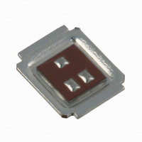
MOSFET N-CH 100V DIRECTFET-MN
Manufacturer
International Rectifier
Series
HEXFET®r
Datasheet
1.IRF6644.pdf
(10 pages)
Specifications of IRF6644
Fet Type
MOSFET N-Channel, Metal Oxide
Fet Feature
Standard
Rds On (max) @ Id, Vgs
13 mOhm @ 10.3A, 10V
Drain To Source Voltage (vdss)
100V
Current - Continuous Drain (id) @ 25° C
10.3A
Vgs(th) (max) @ Id
4.8V @ 150µA
Gate Charge (qg) @ Vgs
47nC @ 10V
Input Capacitance (ciss) @ Vds
2210pF @ 25V
Power - Max
2.8W
Mounting Type
Surface Mount
Package / Case
DirectFET™ Isometric MN
Configuration
Single Quad Drain Dual Source
Transistor Polarity
N-Channel
Resistance Drain-source Rds (on)
13 m Ohms
Drain-source Breakdown Voltage
100 V
Gate-source Breakdown Voltage
+/- 20 V
Continuous Drain Current
10.3 A
Power Dissipation
2.8 W
Maximum Operating Temperature
+ 150 C
Mounting Style
Through Hole
Fall Time
16 ns
Minimum Operating Temperature
- 40 C
Rise Time
26 ns
Lead Free Status / Rohs Status
No
Available stocks
Company
Part Number
Manufacturer
Quantity
Price
Company:

Part Number:
IRF6644MDF2
Manufacturer:
MOLEX
Quantity:
1 454
Part Number:
IRF6644MDF2
Manufacturer:
IR
Quantity:
20 000
Part Number:
IRF6644TR1
Manufacturer:
IR
Quantity:
20 000
Part Number:
IRF6644TR1PBF
Manufacturer:
IR
Quantity:
20 000


‚
Notes:
IRF6644
Static @ T
BV
∆ΒV
R
V
∆V
I
I
gfs
Q
Q
Q
R
t
t
t
t
C
C
C
C
C
Diode Characteristics
I
I
V
t
Q
DSS
GSS
d(on)
r
d(off)
f
S
SM
rr
GS(th)
SD
DS(on)
G
iss
oss
rss
oss
oss
g
Q
Q
Q
Q
sw
oss
rr
Pulse width ≤ 400µs; duty cycle ≤ 2%.
Repetitive rating; pulse width limited by max. junction temperature.
2
GS(th)
DSS
gs1
gs2
gd
godr
DSS
/∆T
/∆T
J
J
J
= 25°C (unless otherwise specified)
Drain-to-Source Breakdown Voltage
Breakdown Voltage Temp. Coefficient
Static Drain-to-Source On-Resistance
Gate Threshold Voltage
Gate Threshold Voltage Coefficient
Drain-to-Source Leakage Current
Gate-to-Source Forward Leakage
Gate-to-Source Reverse Leakage
Forward Transconductance
Total Gate Charge
Pre-Vth Gate-to-Source Charge
Post-Vth Gate-to-Source Charge
Gate-to-Drain Charge
Gate Charge Overdrive
Switch Charge (Q
Output Charge
Gate Resistance
Turn-On Delay Time
Rise Time
Turn-Off Delay Time
Fall Time
Input Capacitance
Output Capacitance
Reverse Transfer Capacitance
Output Capacitance
Output Capacitance
Continuous Source Current
(Body Diode)
Pulsed Source Current
(Body Diode) d
Diode Forward Voltage
Reverse Recovery Time
Reverse Recovery Charge
Parameter
Parameter
gs2
+ Q
gd
)
Min. Typ. Max. Units
Min. Typ. Max. Units
100
–––
–––
–––
–––
–––
–––
–––
–––
–––
–––
–––
–––
–––
–––
–––
–––
–––
–––
–––
–––
–––
–––
–––
–––
–––
–––
–––
–––
2.8
–––
15
2210
2120
0.11
10.3
11.5
13.1
–––
–––
–––
–––
–––
–––
–––
420
100
240
–––
–––
–––
-10
8.0
1.6
1.0
35
13
17
17
26
34
16
42
69
-100
17.3
–––
–––
–––
250
100
–––
–––
–––
–––
–––
–––
–––
–––
–––
–––
–––
–––
–––
–––
–––
100
4.8
2.0
1.3
13
20
47
10
82
63
mV/°C
V/°C
mΩ
µA
nA
nC
nC
nC
pF
ns
ns
V
V
S
Ω
A
V
V
Reference to 25°C, I
V
V
V
V
V
V
V
V
V
I
See Fig. 17
V
V
I
R
V
V
ƒ = 1.0MHz
V
V
MOSFET symbol
showing the
integral reverse
p-n junction diode.
T
T
di/dt = 100A/µs c
D
D
J
J
GS
GS
DS
DS
DS
GS
GS
DS
DS
GS
DS
DD
GS
DS
GS
GS
G
= 6.2A
= 6.2A
=6.2Ω
= 25°C, I
= 25°C, I
= V
= 100V, V
= 80V, V
= 10V, I
= 50V
= 16V, V
= 25V
= 0V, I
= 10V, I
= 20V
= -20V
= 10V
= 50V, V
= 0V
= 0V, V
= 0V, V
GS
, I
D
Conditions
D
Conditions
S
F
DS
DS
D
D
= 250µA
GS
GS
GS
= 6.2A, V
= 6.2A, V
= 150µA
= 10.3A c
= 6.2A
GS
= 1.0V, f=1.0MHz
= 80V, f=1.0MHz
= 0V, T
= 0V
= 10V c
= 0V
D
www.irf.com
= 1mA
DD
GS
J
= 125°C
= 0V c
= 50V
Related parts for IRF6644
Image
Part Number
Description
Manufacturer
Datasheet
Request
R

Part Number:
Description:
SCHOTTKY RECTIFIER
Manufacturer:
International Rectifier Corp.
Datasheet:
Part Number:
Description:
SCHOTTKY RECTIFIER
Manufacturer:
International Rectifier Corp.
Datasheet:
Part Number:
Description:
SCHOTTKY RECTIFIER
Manufacturer:
International Rectifier Corp.
Datasheet:
Part Number:
Description:
SCHOTTKY RECTIFIER
Manufacturer:
International Rectifier Corp.
Datasheet:
Part Number:
Description:
SCHOTTKY RECTIFIER
Manufacturer:
International Rectifier Corp.
Datasheet:
Part Number:
Description:
SCHOTTKY RECTIFIER
Manufacturer:
International Rectifier Corp.
Datasheet:
Part Number:
Description:
SCHOTTKY RECTIFIER
Manufacturer:
International Rectifier Corp.
Datasheet:
Part Number:
Description:
SCHOTTKY RECTIFIER
Manufacturer:
International Rectifier Corp.
Datasheet:
Part Number:
Description:
SCHOTTKY RECTIFIER
Manufacturer:
International Rectifier Corp.
Datasheet:
Part Number:
Description:
SCHOTTKY RECTIFIER
Manufacturer:
International Rectifier Corp.
Datasheet:
Part Number:
Description:
SCHOTTKY RECTIFIER
Manufacturer:
International Rectifier Corp.
Datasheet:
Part Number:
Description:
SCHOTTKY RECTIFIER
Manufacturer:
International Rectifier Corp.
Datasheet:
Part Number:
Description:
SCHOTTKY RECTIFIER
Manufacturer:
International Rectifier Corp.
Datasheet:
Part Number:
Description:
SCHOTTKY RECTIFIER
Manufacturer:
International Rectifier Corp.
Datasheet:
Part Number:
Description:
SCHOTTKY RECTIFIER
Manufacturer:
International Rectifier Corp.
Datasheet: