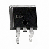
IRF1404ZSPBF International Rectifier, IRF1404ZSPBF Datasheet - Page 4

IRF1404ZSPBF
Manufacturer Part Number
IRF1404ZSPBF
Description
MOSFET N-CH 40V 75A D2PAK
Manufacturer
International Rectifier
Series
HEXFET®r
Type
Power MOSFETr
Specifications of IRF1404ZSPBF
Fet Type
MOSFET N-Channel, Metal Oxide
Fet Feature
Standard
Rds On (max) @ Id, Vgs
3.7 mOhm @ 75A, 10V
Drain To Source Voltage (vdss)
40V
Current - Continuous Drain (id) @ 25° C
75A
Vgs(th) (max) @ Id
4V @ 250µA
Gate Charge (qg) @ Vgs
150nC @ 10V
Input Capacitance (ciss) @ Vds
4340pF @ 25V
Power - Max
200W
Mounting Type
Surface Mount
Package / Case
D²Pak, TO-263 (2 leads + tab)
Current, Drain
200 A
Gate Charge, Total
75 nC
Package Type
D2Pak
Polarization
N-Channel
Power Dissipation
230 W
Resistance, Drain To Source On
2.7 Milliohms
Temperature, Operating, Maximum
+175 °C
Temperature, Operating, Minimum
-55 °C
Time, Turn-off Delay
30 ns
Time, Turn-on Delay
19 ns
Transconductance, Forward
170 S
Voltage, Breakdown, Drain To Source
40 V
Voltage, Forward, Diode
1.3 V
Voltage, Gate To Source
±16 V
Transistor Polarity
N Channel
Continuous Drain Current Id
75A
Drain Source Voltage Vds
40V
On Resistance Rds(on)
3.7mohm
Rds(on) Test Voltage Vgs
10V
Threshold Voltage Vgs Typ
4V
Rohs Compliant
Yes
Number Of Elements
1
Polarity
N
Channel Mode
Enhancement
Drain-source On-res
0.0037Ohm
Drain-source On-volt
40V
Gate-source Voltage (max)
±20V
Continuous Drain Current
190A
Operating Temp Range
-55C to 175C
Operating Temperature Classification
Military
Mounting
Surface Mount
Pin Count
2 +Tab
Lead Free Status / RoHS Status
Lead free / RoHS Compliant
Available stocks
Company
Part Number
Manufacturer
Quantity
Price
Company:
Part Number:
IRF1404ZSPBF
Manufacturer:
AMD
Quantity:
4 219
4
1000.0
100.0
8000
6000
4000
2000
10.0
1.0
0.1
0
Fig 5. Typical Capacitance Vs.
Fig 7. Typical Source-Drain Diode
0.2
1
Drain-to-Source Voltage
T J = 175°C
V DS , Drain-to-Source Voltage (V)
V SD , Source-toDrain Voltage (V)
Forward Voltage
V GS = 0V,
C iss = C gs + C gd , C ds SHORTED
C rss = C gd
C oss = C ds + C gd
0.6
Crss
Ciss
Coss
T J = 25°C
1.0
f = 1 MHZ
10
1.4
V GS = 0V
1.8
100
10000
1000
100
Fig 8. Maximum Safe Operating Area
10
20
16
12
8
4
0
1
Fig 6. Typical Gate Charge Vs.
0
0
Tc = 25°C
Tj = 175°C
Single Pulse
I D = 75A
Gate-to-Source Voltage
V DS , Drain-toSource Voltage (V)
Q G Total Gate Charge (nC)
40
1
OPERATION IN THIS AREA
LIMITED BY R DS (on)
V DS = 32V
VDS= 20V
10
80
www.irf.com
100µsec
10msec
1msec
120
100
1000
160


