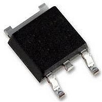
STB200N4F3 STMicroelectronics, STB200N4F3 Datasheet - Page 3

STB200N4F3
Manufacturer Part Number
STB200N4F3
Description
MOSFET N-CH 40V 120A D2PAK
Manufacturer
STMicroelectronics
Series
STripFET™r
Datasheet
1.STP200N4F3.pdf
(14 pages)
Specifications of STB200N4F3
Fet Type
MOSFET N-Channel, Metal Oxide
Fet Feature
Standard
Rds On (max) @ Id, Vgs
4 mOhm @ 80A, 10V
Drain To Source Voltage (vdss)
40V
Current - Continuous Drain (id) @ 25° C
120A
Vgs(th) (max) @ Id
4V @ 250µA
Gate Charge (qg) @ Vgs
75nC @ 10V
Input Capacitance (ciss) @ Vds
5100pF @ 25V
Power - Max
300W
Mounting Type
Surface Mount
Package / Case
D²Pak, TO-263 (2 leads + tab)
Transistor Polarity
N Channel
Continuous Drain Current Id
60A
Drain Source Voltage Vds
40V
On Resistance Rds(on)
2.5mohm
Rds(on) Test Voltage Vgs
10V
Threshold Voltage Vgs Typ
4V
Rohs Compliant
Yes
Configuration
Single
Resistance Drain-source Rds (on)
0.0031 Ohms
Drain-source Breakdown Voltage
40 V
Gate-source Breakdown Voltage
+/- 20 V
Continuous Drain Current
120 A
Power Dissipation
300 W
Maximum Operating Temperature
+ 175 C
Mounting Style
SMD/SMT
Minimum Operating Temperature
- 55 C
Lead Free Status / RoHS Status
Lead free / RoHS Compliant
Available stocks
Company
Part Number
Manufacturer
Quantity
Price
Company:
Part Number:
STB200N4F3
Manufacturer:
ST
Quantity:
12 500
STB200N4F3, STP200N4F3
1
Electrical ratings
Table 2.
1. Current limited by package
2. Pulse width limited by safe operating area
3. Starting Tj = 25°C, I
4. I
Table 3.
1. When mounted on FR-4 board, 1inch² 2 oz. Cu.
R
Symbol
Symbol
thJ-PCB
dv/dt
E
I
R
R
SD
DM
P
I
I
V
V
AS
T
D
D
T
thJC
thJA
TOT
GS
DS
stg
(1)
(1)
≤ 60A, di/dt ≤ 440 A/µs, V
J
(2)
(3)
(4)
(1)
Absolute maximum ratings
Thermal data
Thermal resistance junction-case max
Thermal resistance junction-pcb max
Thermal resistance junction-ambient max
Drain-source voltage
Gate-source voltage
Drain current (continuous) at T
Drain current (continuous) at T
Drain current (pulsed)
Total dissipation at T
Derating factor
Single pulse avalanche energy
Peak diode recovery voltage slope
Operating junction temperature
Storage temperature
D
= 60A, V
DD
DD
≤ V
= 25V
Parameter
Parameter
(BR)DSS
Doc ID 13302 Rev 3
C
= 25 °C
, T
j
≤ T
C
C
JMAX.
= 25 °C
= 100 °C
TO-220
62.5
-55 to 175
Value
Value
0.50
±20
120
120
480
300
862
2.0
4.2
40
Electrical ratings
D²PAK
35
W/°C
°C/W
°C/W
°C/W
Unit
V/ns
Unit
mJ
°C
W
V
V
A
A
A
3/14


