IRFS3006-7PPBF International Rectifier, IRFS3006-7PPBF Datasheet - Page 2
IRFS3006-7PPBF
Manufacturer Part Number
IRFS3006-7PPBF
Description
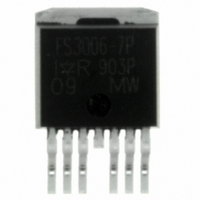
MOSFET N-CH 60V 240A D2PAK-7
Manufacturer
International Rectifier
Series
HEXFET®r
Datasheet
1.IRFS3006TRL7PP.pdf
(9 pages)
Specifications of IRFS3006-7PPBF
Fet Type
MOSFET N-Channel, Metal Oxide
Fet Feature
Standard
Rds On (max) @ Id, Vgs
2.1 mOhm @ 168A, 10V
Drain To Source Voltage (vdss)
60V
Current - Continuous Drain (id) @ 25° C
240A
Vgs(th) (max) @ Id
4V @ 250µA
Gate Charge (qg) @ Vgs
300nC @ 10V
Input Capacitance (ciss) @ Vds
8850pF @ 50V
Power - Max
375W
Mounting Type
Surface Mount
Package / Case
D²Pak, TO-263 (6 leads + tab)
Transistor Polarity
N-Channel
Drain-source Breakdown Voltage
60 V
Gate-source Breakdown Voltage
20 V
Continuous Drain Current
293 A
Power Dissipation
375 W
Mounting Style
SMD/SMT
Gate Charge Qg
200 nC
Lead Free Status / RoHS Status
Lead free / RoHS Compliant


∆V
Notes:
‚
ƒ
„
Static @ T
V
R
V
I
I
R
Dynamic @ T
gfs
Q
Q
Q
Q
t
t
t
t
C
C
C
C
C
Diode Characteristics
I
I
V
t
Q
I
t
DSS
GSS
d(on)
r
d(off)
f
S
SM
rr
RRM
on
(BR)DSS
GS(th)
SD
DS(on)
G(int)
iss
oss
rss
oss
oss
some lead mounting arrangements.
g
gs
gd
sync
rr
limitation arising from heating of the device leds may occur with
Calcuted continuous current based on maximum allowable junction
Repetitive rating; pulse width limited by max. junction
Limited by T
2
Symbol
Symbol
Symbol
temperature.
I
(BR)DSS
temperature Bond wire current limit is 240A. Note that current
R
SD
above this value .
G
eff. (ER) Effective Output Capacitance (Energy Related)
eff. (TR) Effective Output Capacitance (Time Related)
≤ 168A, di/dt ≤ 1410 A/µs, V
= 25Ω, I
/∆T
J
AS
J
Jmax
Drain-to-Source Breakdown Voltage
Breakdown Voltage Temp. Coefficient
Static Drain-to-Source On-Resistance
Gate Threshold Voltage
Drain-to-Source Leakage Current
Gate-to-Source Forward Leakage
Gate-to-Source Reverse Leakage
Internal Gate Resistance
Forward Transconductance
Total Gate Charge
Gate-to-Source Charge
Gate-to-Drain ("Miller") Charge
Total Gate Charge Sync. (Q
Turn-On Delay Time
Rise Time
Turn-Off Delay Time
Fall Time
Input Capacitance
Output Capacitance
Reverse Transfer Capacitance
Continuous Source Current
(Body Diode)
Pulsed Source Current
(Body Diode)
Diode Forward Voltage
Reverse Recovery Time
Reverse Recovery Charge
Reverse Recovery Current
Forward Turn-On Time
= 25°C (unless otherwise specified)
= 168A, V
, starting T
J
= 25°C (unless otherwise specified)
Parameter
GS
J
=10V. Part not recommended for use
= 25°C, L = 0.021mH
Ãd
DD
≤ V
Parameter
Parameter
(BR)DSS
, T
g
- Q
J
≤ 175°C.
gd
)
h
Ã
Intrinsic turn-on time is negligible (turn-on is dominated by LS+LD)
Min. Typ. Max. Units
Min. Typ. Max. Units
Min. Typ. Max. Units
–––
–––
–––
–––
–––
–––
290
–––
–––
–––
–––
–––
–––
–––
–––
–––
–––
–––
–––
–––
–––
–––
–––
–––
–––
–––
–––
–––
–––
2.0
…
†
‡
ˆ
‰
Š
60
Pulse width ≤ 400µs; duty cycle ≤ 2%.
C
When mounted on 1" square PCB (FR-4 or G-10 Material). For
C
as C
C
note # AN-994 echniques refer to application note #AN-994.
recommended footprint and soldering techniquea refer to applocation
θJC
oss
θ
oss
oss
8850
1007
1460
1915
0.07
2.03
–––
–––
–––
–––
–––
–––
–––
200
140
118
525
–––
–––
–––
1.5
eff. (TR) is a fixed capacitance that gives the same charging time
oss
2.1
eff. (ER) is a fixed capacitance that gives the same energy as
while V
37
60
14
61
69
44
48
51
62
while V
293
1172
-100
DS
–––
–––
250
100
–––
–––
300
–––
–––
–––
–––
–––
–––
–––
–––
–––
–––
–––
–––
–––
–––
–––
–––
–––
2.1
4.0
1.3
20
is rising from 0 to 80% V
DS
™
is rising from 0 to 80% V
V/°C
mΩ
nC
nC
µA
nA
pF
ns
ns
V
V
Ω
S
A
V
A
V
Reference to 25°C, I
V
V
V
V
V
V
V
I
V
V
I
V
I
R
V
V
V
ƒ = 1.0MHz (See Fig 5)
V
V
MOSFET symbol
showing the
integral reverse
p-n junction diode.
T
T
T
T
T
T
D
D
D
J
J
J
J
J
J
GS
GS
DS
DS
DS
GS
GS
DS
DS
GS
DD
GS
GS
DS
GS
GS
G
= 168A
= 168A, V
= 168A
= 25°C, I
= 25°C
= 125°C
= 25°C
= 125°C
= 25°C
= 2.7Ω
= V
= 60V, V
= 60V, V
= 25V, I
= 30V
= 50V
= 0V, I
= 10V, I
= 20V
= -20V
= 10V
= 39V
= 10V
= 0V
= 0V, V
= 0V, V
GS
, I
D
g
g
S
D
DS
DS
DSS
D
D
DS
= 250µA
GS
GS
= 168A, V
= 250µA
= 168A
= 168A
= 0V to 48V
= 0V to 48V
Conditions
Conditions
Conditions
DSS
.
=0V, V
= 0V
= 0V, T
V
I
di/dt = 100A/µs
.
F
R
= 168A
D
= 51V,
g
GS
= 5mA
J
GS
= 125°C
= 10V
= 0V
h
www.irf.com
G
d
(See Fig 11)
g
g
S
D
Related parts for IRFS3006-7PPBF
Image
Part Number
Description
Manufacturer
Datasheet
Request
R

Part Number:
Description:
SCHOTTKY RECTIFIER
Manufacturer:
International Rectifier Corp.
Datasheet:
Part Number:
Description:
SCHOTTKY RECTIFIER
Manufacturer:
International Rectifier Corp.
Datasheet:
Part Number:
Description:
SCHOTTKY RECTIFIER
Manufacturer:
International Rectifier Corp.
Datasheet:
Part Number:
Description:
SCHOTTKY RECTIFIER
Manufacturer:
International Rectifier Corp.
Datasheet:
Part Number:
Description:
SCHOTTKY RECTIFIER
Manufacturer:
International Rectifier Corp.
Datasheet:
Part Number:
Description:
SCHOTTKY RECTIFIER
Manufacturer:
International Rectifier Corp.
Datasheet:
Part Number:
Description:
SCHOTTKY RECTIFIER
Manufacturer:
International Rectifier Corp.
Datasheet:
Part Number:
Description:
SCHOTTKY RECTIFIER
Manufacturer:
International Rectifier Corp.
Datasheet:
Part Number:
Description:
SCHOTTKY RECTIFIER
Manufacturer:
International Rectifier Corp.
Datasheet:
Part Number:
Description:
SCHOTTKY RECTIFIER
Manufacturer:
International Rectifier Corp.
Datasheet:
Part Number:
Description:
SCHOTTKY RECTIFIER
Manufacturer:
International Rectifier Corp.
Datasheet:
Part Number:
Description:
SCHOTTKY RECTIFIER
Manufacturer:
International Rectifier Corp.
Datasheet:
Part Number:
Description:
SCHOTTKY RECTIFIER
Manufacturer:
International Rectifier Corp.
Datasheet:
Part Number:
Description:
SCHOTTKY RECTIFIER
Manufacturer:
International Rectifier Corp.
Datasheet:
Part Number:
Description:
SCHOTTKY RECTIFIER
Manufacturer:
International Rectifier Corp.
Datasheet: