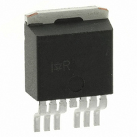
IRF1324S-7PPBF International Rectifier, IRF1324S-7PPBF Datasheet - Page 6

IRF1324S-7PPBF
Manufacturer Part Number
IRF1324S-7PPBF
Description
MOSFET N-CH 24V 429A D2PAK-7
Manufacturer
International Rectifier
Series
HEXFET®r
Type
Power MOSFETr
Datasheet
1.IRF1324STRL-7PP.pdf
(9 pages)
Specifications of IRF1324S-7PPBF
Fet Type
MOSFET N-Channel, Metal Oxide
Fet Feature
Standard
Rds On (max) @ Id, Vgs
1 mOhm @ 160A, 10V
Drain To Source Voltage (vdss)
24V
Current - Continuous Drain (id) @ 25° C
429A
Vgs(th) (max) @ Id
4V @ 250µA
Gate Charge (qg) @ Vgs
252nC @ 10V
Input Capacitance (ciss) @ Vds
7700pF @ 19V
Power - Max
300W
Mounting Type
Surface Mount
Package / Case
D²Pak, TO-263 (6 leads + tab)
Number Of Elements
1
Polarity
N
Channel Mode
Enhancement
Drain-source On-res
0.001Ohm
Drain-source On-volt
24V
Gate-source Voltage (max)
±20V
Drain Current (max)
429A
Power Dissipation
300W
Output Power (max)
Not RequiredW
Frequency (max)
Not RequiredMHz
Noise Figure
Not RequireddB
Power Gain
Not RequireddB
Drain Efficiency
Not Required%
Operating Temp Range
-55C to 175C
Operating Temperature Classification
Military
Mounting
Surface Mount
Pin Count
6 +Tab
Package Type
D2PAK
Transistor Polarity
N-Channel
Drain-source Breakdown Voltage
24 V
Gate-source Breakdown Voltage
20 V
Continuous Drain Current
429 A
Mounting Style
SMD/SMT
Gate Charge Qg
180 nC
Lead Free Status / RoHS Status
Lead free / RoHS Compliant
Available stocks
Company
Part Number
Manufacturer
Quantity
Price
Part Number:
IRF1324S-7PPBF
Manufacturer:
IR
Quantity:
20 000
6
Fig 15. Maximum Avalanche Energy vs. Temperature
250
200
150
100
50
0
25
Starting T J , Junction Temperature (°C)
50
TOP
BOTTOM 1.0% Duty Cycle
I D = 160A
75
100
Single Pulse
125
4.5
4.0
3.5
3.0
2.5
2.0
1.5
1.0
Fig 16. Threshold Voltage Vs. Temperature
150
-75 -50 -25 0
I D = 250µA
I D = 1.0mA
I D = 1.0A
175
T J , Temperature ( °C )
25 50 75 100 125 150 175 200
Notes on Repetitive Avalanche Curves , Figures 14, 15:
(For further info, see AN-1005 at www.irf.com)
1. Avalanche failures assumption:
2. Safe operation in Avalanche is allowed as long asT
3. Equation below based on circuit and waveforms shown in Figures 16a, 16b.
4. P
5. BV = Rated breakdown voltage (1.3 factor accounts for voltage increase
6. I
7. ∆T
Purely a thermal phenomenon and failure occurs at a temperature far in
excess of T
during avalanche).
25°C in Figure 14, 15).
t
D = Duty cycle in avalanche = t
Z
av
av =
thJC
D (ave)
= Allowable avalanche current.
=
Average time in avalanche.
(D, t
Allowable rise in junction temperature, not to exceed T
= Average power dissipation per single avalanche pulse.
av
) = Transient thermal resistance, see Figures 13)
jmax
. This is validated for every part type.
P
D (ave)
= 1/2 ( 1.3·BV·I
I
E
av
AS (AR)
= 2DT/ [1.3·BV·Z
av
·f
= P
D (ave)
av
) = DT/ Z
·t
th
av
]
jmax
thJC
jmax
is not exceeded.
www.irf.com
(assumed as


