NTD2955G ON Semiconductor, NTD2955G Datasheet

MOSFET P-CH 60V 12A DPAK

NTD2955G

Manufacturer Part Number
NTD2955G
Description
MOSFET P-CH 60V 12A DPAK
Manufacturer
ON Semiconductor
Datasheet

Specifications of NTD2955G

Fet Type
MOSFET P-Channel, Metal Oxide
Fet Feature
Standard
Rds On (max) @ Id, Vgs
180 mOhm @ 6A, 10V
Drain To Source Voltage (vdss)
60V
Current - Continuous Drain (id) @ 25° C
12A
Vgs(th) (max) @ Id
4V @ 250µA
Gate Charge (qg) @ Vgs
30nC @ 10V
Input Capacitance (ciss) @ Vds
750pF @ 25V
Power - Max
55W
Mounting Type
Surface Mount
Package / Case
DPak, TO-252 (2 leads+tab), SC-63
Configuration
Single
Transistor Polarity
P-Channel
Resistance Drain-source Rds (on)
0.18 Ohm @ 10 V
Forward Transconductance Gfs (max / Min)
8 S
Drain-source Breakdown Voltage
60 V
Gate-source Breakdown Voltage
+/- 20 V
Continuous Drain Current
12 A
Power Dissipation
55000 mW
Maximum Operating Temperature
+ 175 C
Mounting Style
SMD/SMT
Minimum Operating Temperature
- 55 C
Lead Free Status / RoHS Status
Lead free / RoHS Compliant
Other names
NTD2955G
NTD2955GOS

Available stocks

Company
Part Number
Manufacturer
Quantity
Price
Part Number:
NTD2955G
Manufacturer:
ON
Quantity:
12 500
Part Number:
NTD2955G
Manufacturer:
ON SEMICONDUCTOR
Quantity:
30 000
Part Number:
NTD2955G
Manufacturer:
ON
Quantity:
12 500
NTD2955, NTD2955P
Power MOSFET
avalanche and commutation modes. Designed for low-voltage, high-
speed switching applications in power supplies, converters, and power
motor controls. These devices are particularly well suited for bridge
circuits where diode speed and commutating safe operating areas are
critical and offer an additional safety margin against unexpected
voltage transients.
Features
Stresses exceeding Maximum Ratings may damage the device. Maximum
Ratings are stress ratings only. Functional operation above the Recommended
Operating Conditions is not implied. Extended exposure to stresses above the
Recommended Operating Conditions may affect device reliability.
1. When surface mounted to an FR4 board using 1 in pad size
2. When surface mounted to an FR4 board using the minimum recommended
© Semiconductor Components Industries, LLC, 2008
January, 2008 - Rev. 9
-60 V, -12 A, P-Channel DPAK
MAXIMUM RATINGS
Drain-to-Source Voltage
Gate-to-Source Voltage
Drain Current
Drain Current
Drain Current
Total Power Dissipation @ T
Operating and Storage Temperature
Single Pulse Drain-to-Source Avalanche
Thermal Resistance
Maximum Lead Temperature for Soldering
This Power MOSFET is designed to withstand high energy in the
to Withstand High Energy in the Avalanche and Commutation Modes
Avalanche Energy Specified
I
Designed for Low-Voltage, High-Speed Switching Applications and
Pb-Free Packages are Available
(Cu area = 1.127 in
pad size (Cu area = 0.412 in
DSS
- Continuous
- Non-repetitive (t
Range
Energy - Starting T
(V
I
- Junction-to-Case
- Junction-to-Ambient (Note 1)
- Junction-to-Ambient (Note 2)
Purposes, 1/8 in. from case for
10 seconds
L
DD
= 12 Apk, L = 3.0 mH, R
and V
= 25 Vdc, V
DS(on)
- Continuous @ T
- Single Pulse (t
Rating
GS
2
Specified at Elevated Temperature
p
).
J
≤ 10 ms)
= 10 Vdc, Peak
= 25°C
(T
J
= 25°C unless otherwise noted)
a
G
= 25°C
2
p
= 25 W)
).
a
≤ 10 ms)
= 25°C
Symbol
T
V
V
R
R
R
V
J
E
I
P
GSM
, T
DSS
DM
T
I
qJC
qJA
qJA
GS
AS
D
D
L
stg
- 55 to
Value
± 20
± 25
2.73
71.4
-60
-12
-36
175
216
100
260
55
1
°C/W
Unit
Vdc
Vdc
Vpk
Adc
Apk
mJ
°C
°C
W
See detailed ordering and shipping information in the package
dimensions section on page 6 of this data sheet.
CASE 369C
V
STYLE 2
1 2
(BR)DSS
-60 V
DPAK
CASE 369D
1
3
STYLE 2
DPAK-3
2
3
ORDERING INFORMATION
Gate
G
4
155 mW @ -10 V, 6 A
Y
WW
G
http://onsemi.com
4
1
R
Drain
MARKING DIAGRAMS
Drain
DS(on)
4
2
= Year
= Work Week
= Pb-Free Package
P-Channel
D
3
Source
Publication Order Number:
TYP
S
Gate
Gate
1
1
Drain
Drain
Drain
Drain
NTD2955/D
4
2
I
4
2
D
-12 A
MAX
3
Source
3
Source

Related parts for NTD2955G

NTD2955G Summary of contents

Page 1

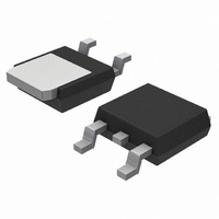
NTD2955, NTD2955P Power MOSFET -60 V, -12 A, P-Channel DPAK This Power MOSFET is designed to withstand high energy in the avalanche and commutation modes. Designed for low-voltage, high- speed switching applications in power supplies, converters, and power motor controls. ...

Page 2

ELECTRICAL CHARACTERISTICS Characteristic OFF CHARACTERISTICS Drain-to-Source Breakdown Voltage (Note Vdc -0.25 mA (Positive Temperature Coefficient) Zero Gate Voltage Drain Current ( Vdc -60 Vdc 25°C) GS ...

Page 3

TYPICAL PERFORMANCE CURVES - 25° -9 DRAIN-TO-SOURCE VOLTAGE (VOLTS) DS Figure 1. On-Region Characteristics 0.50 ...

Page 4

1000 iss C rss 800 600 400 200 GATE-TO-SOURCE OR DRAIN-TO-SOURCE VOLTAGE (V) Figure 7. Capacitance Variation 1000 ...

Page 5

D = 0.5 0.2 0.1 0.05 0.1 0.02 0.01 SINGLE PULSE 0.01 1.0E-05 1.0E-04 1.0E-03 NTD2955, NTD2955P P (pk DUTY CYCLE 1.0E-02 1.0E-01 t, TIME (s) Figure 13. Thermal Response http://onsemi.com 5 ...

Page 6

... ORDERING INFORMATION Device NTD2955 NTD2955G NTD2955-001 NTD2955-1G NTD2955T4 NTD2955T4G NTD2955PT4G †For information on tape and reel specifications, including part orientation and tape sizes, please refer to our Tape and Reel Packaging Specifications Brochure, BRD8011/D. NTD2955, NTD2955P Package DPAK DPAK (Pb-Free) DPAK-3 DPAK-3 (Pb-Free) ...

Page 7

... 0.13 (0.005) M 5.80 0.228 *For additional information on our Pb-Free strategy and soldering details, please download the ON Semiconductor Soldering and Mounting Techniques Reference Manual, SOLDERRM/D. NTD2955, NTD2955P PACKAGE DIMENSIONS DPAK CASE 369C-01 ISSUE O SEATING -T- PLANE SOLDERING FOOTPRINT* 6.20 3.0 0.244 0.118 2.58 ...

Page 8

... G 0.13 (0.005) *For additional information on our Pb-Free strategy and soldering details, please download the ON Semiconductor Soldering and Mounting Techniques Reference Manual, SOLDERRM/D. ON Semiconductor and are registered trademarks of Semiconductor Components Industries, LLC (SCILLC). SCILLC reserves the right to make changes without further notice to any products herein ...

Related keywords