FDH50N50 Fairchild Semiconductor, FDH50N50 Datasheet
FDH50N50
Specifications of FDH50N50
Available stocks


Related parts for FDH50N50


FDH50N50 Summary of contents
Page 1
... Thermal Resistance, Case-to-Sink CS R Thermal Resistance, Junction-to-Ambient JA ©2004 Fairchild Semiconductor Corporation FDH50N50 / FDA50N50 Rev. A Description = 10 V These N-Channel enhancement mode power field effect transis- tors are produced using Fairchild’s proprietary, planar stripe, DMOS technology. This advanced technology has been especially tailored to mini- ...
Page 2
... Repetitive Rating: Pulse width limited by maximum junction temperature 1.46mH 48A 50V Starting 48A, di/dt 200A Starting DSS 4. Pulse Test: Pulse width 300 s, Duty Cycle 5. Essentially Independent of Operating Temperature Typical Characteristics FDH50N50 / FDA50N50 Rev. A Package Reel Size TO-247 - TO- 25°C unless otherwise noted C Conditions 250 250 A, Referenced ...
Page 3
... V GS 0.2 0.1 0 Drain Current [A] D Figure 5. Capacitance Characteristics 12,000 10,000 8,000 6,000 4,000 2,000 C rss Drain-Source Voltage [V] DS FDH50N50 / FDA50N50 Rev. A Figure 2. Transfer Characteristics 100 10 1 Notes : 1. 250 s Pulse Test 0 Figure 4. Body Diode Forward Voltage 160 120 = 10V 20V Note : ...
Page 4
... Figure 11. Typical Drain Current Slope vs. Gate Resistance 4,000 3,500 3,000 2,500 di/dt(on) 2,000 1,500 di/dt(off) 1,000 500 Gate resistance [ ] G FDH50N50 / FDA50N50 Rev. A (Continued) Figure 8. On-Resistance Variation 2.5 2.0 1.5 1.0 Notes : 0 250 A D 0.0 100 150 200 -100 o C] Figure 10. Maximum Drain Current ...
Page 5
... Typical Performance Characteristics Figure 13. Typical Switching Losses vs. Gate Resistance 1,000 800 600 400 200 Gate resistance [ ] G Figure 15. Transient Thermal Resistance Curve FDH50N50 / FDA50N50 Rev. A (Continued) Figure 14. Unclamped Inductive Switching 100 Eoff 10 Eon Notes : 400 25A 125 0.01 D=0.5 -1 0.2 Notes : 1. Z 0.1 2 ...
Page 6
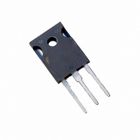
... Mechanical Dimensions TO-247AD (FKS PKG CODE 001) FDH50N50 / FDA50N50 Rev. A Dimensions in Millimeters 6 www.fairchildsemi.com ...
Page 7
... Mechanical Dimensions ø3.20 0.10 2.00 0.20 3.00 0.20 1.00 0.20 5.45TYP [5.45 ] 0.30 FDH50N50 / FDA50N50 Rev. A (Continued) TO-3P 15.60 0.20 13.60 0.20 9.60 0.20 5.45TYP [5.45 ] 0.30 7 4.80 0.20 +0.15 1.50 –0.05 1.40 0.20 +0.15 0.60 –0.05 Dimensions in Millimeters www.fairchildsemi.com ...
Page 8
... PRODUCT STATUS DEFINITIONS Definition of Terms Datasheet Identification Advance Information Preliminary No Identification Needed Obsolete FDH50N50 / FDA50N50 Rev. A ISOPLANAR™ Power247™ LittleFET™ PowerEdge™ MICROCOUPLER™ PowerSaver™ MicroFET™ PowerTrench MicroPak™ ...