HUF75343G3 Fairchild Semiconductor, HUF75343G3 Datasheet - Page 2
HUF75343G3
Manufacturer Part Number
HUF75343G3
Description
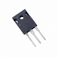
MOSFET N-CH 55V 75A TO-247
Manufacturer
Fairchild Semiconductor
Series
UltraFET™r
Datasheet
1.HUF75343S3ST.pdf
(10 pages)
Specifications of HUF75343G3
Fet Type
MOSFET N-Channel, Metal Oxide
Fet Feature
Standard
Rds On (max) @ Id, Vgs
9 mOhm @ 75A, 10V
Drain To Source Voltage (vdss)
55V
Current - Continuous Drain (id) @ 25° C
75A
Vgs(th) (max) @ Id
4V @ 250µA
Gate Charge (qg) @ Vgs
205nC @ 20V
Input Capacitance (ciss) @ Vds
3000pF @ 25V
Power - Max
270W
Mounting Type
Through Hole
Package / Case
TO-247-3
Lead Free Status / RoHS Status
Lead free / RoHS Compliant
Available stocks
Company
Part Number
Manufacturer
Quantity
Price
Company:

Part Number:
HUF75343G3
Manufacturer:
TOSHIBA
Quantity:
20 000


Absolute Maximum Ratings
Drain to Source Voltage (Note 1) . . . . . . . . . . . . . . . . . . . . . . . V
Drain to Gate Voltage (R
Gate to Source Voltage . . . . . . . . . . . . . . . . . . . . . . . . . . . . . . . V
Drain Current
Pulsed Avalanche Rating . . . . . . . . . . . . . . . . . . . . . . . . . . . . . . E
Power Dissipation . . . . . . . . . . . . . . . . . . . . . . . . . . . . . . . . . . . . P
Operating and Storage Temperature . . . . . . . . . . . . . . . . . .T
Maximum Temperature for Soldering
CAUTION: Stresses above those listed in “Absolute Maximum Ratings” may cause permanent damage to the device. This is a stress only rating and operation of the
device at these or any other conditions above those indicated in the operational sections of this specification is not implied.
NOTE:
Electrical Specifications
©2003 Fairchild Semiconductor Corporation
OFF STATE SPECIFICATIONS
Drain to Source Breakdown Voltage
Zero Gate Voltage Drain Current
Gate to Source Leakage Current
ON STATE SPECIFICATIONS
Gate to Source Threshold Voltage
Drain to Source On Resistance
THERMAL SPECIFICATIONS
Thermal Resistance Junction to Case
Thermal Resistance Junction to Ambient
SWITCHING SPECIFICATIONS (V
Turn-On Time
Turn-On Delay Time
Rise Time
Turn-Off Delay Time
Fall Time
Turn-Off Time
GATE CHARGE SPECIFICATIONS
Total Gate Charge
Gate Charge at 10V
Threshold Gate Charge
Gate to Source Gate Charge
Gate to Drain “Miller” Charge
1. T
Continuous (Figure 2). . . . . . . . . . . . . . . . . . . . . . . . . . . . . . . . . I
Pulsed Drain Current . . . . . . . . . . . . . . . . . . . . . . . . . . . . . . . . I
Derate Above 25
Leads at 0.063in (1.6mm) from Case for 10s. . . . . . . . . . . . . . . T
Package Body for 10s, See Techbrief 334 . . . . . . . . . . . . . . . T
J
= 25
o
C to 150
PARAMETER
o
C . . . . . . . . . . . . . . . . . . . . . . . . . . . . . . . . . . . .
o
C.
GS
= 20k ) (Note 1) . . . . . . . . . . . . . V
T
GS
C
= 25
= 10V)
T
C
= 25
o
C, Unless Otherwise Specified
o
SYMBOL
V
r
Q
C, Unless Otherwise Specified
BV
t
Q
DS(ON)
Q
t
d(OFF)
GS(TH)
R
R
I
I
d(ON)
t
g(TOT)
Q
Q
DSS
GSS
t
OFF
g(TH)
g(10)
ON
DSS
t
t
gd
gs
r
f
JC
JA
J
I
V
V
V
V
I
(Figure 3)
TO-247
TO-220, TO-263
V
R
R
V
V
V
, T
D
D
DS
DS
GS
GS
DD
GS
GS
GS
L
GS
DGR
= 250 A, V
= 75A, V
DSS
STG
= 0.4 , V
pkg
DM
GS
AS
= 50V, V
= 45V, V
= 20V
= V
= 30V, I
= 0V to 20V
= 0V to 10V
= 0V to 2V
= 2.5
D
D
L
DS
, I
GS
TEST CONDITIONS
GS
D
D
GS
GS
GS
= 10V (Figure 9)
= 250 A (Figure 10)
= 0V
= 0V, T
75A,
= 0V (Figure 11)
10V,
V
I
R
I
(Figure 13)
D
g(REF)
DD
L
= 0.4
C
= 30V,
75A,
= 150
= 1.0mA
o
C
HUF75343G3, HUF75343P3, HUF75343S3, HUF75343S3S Rev. B1
MIN
55
-55 to 175
2
-
-
-
-
-
-
-
-
-
-
-
-
-
-
-
-
-
-
Figure 4
Figure 6
1.81
270
300
260
55
55
75
20
0.007
TYP
170
6.0
75
32
18
92
13
42
9
-
-
-
-
-
-
-
-
-
-
0.009
MAX
0.55
250
125
205
110
7.2
100
30
62
75
1
4
-
-
-
-
-
-
-
UNITS
W/
UNITS
o
o
o
o
o
o
W
V
V
V
A
C/W
C/W
C/W
nA
nC
nC
nC
nC
nC
C
C
C
ns
ns
ns
ns
ns
ns
o
V
V
A
A
C
Related parts for HUF75343G3
Image
Part Number
Description
Manufacturer
Datasheet
Request
R

Part Number:
Description:
Fairchild Semiconductor [IGBT MODULE]
Manufacturer:
Fairchild Semiconductor
Datasheet:

Part Number:
Description:
Discrete Semiconductor Modules
Manufacturer:
Fairchild Semiconductor
Part Number:
Description:
Discrete Semiconductor Modules
Manufacturer:
Fairchild Semiconductor
Part Number:
Description:
This N-Channel MOSFET is produced using Fairchild Semiconductor’s advanced Power Trench® process
Manufacturer:
Fairchild Semiconductor
Datasheet:
Part Number:
Description:
This N-Channel MOSFET is produced using Fairchild Semiconductor’s advanced Power Trench® process
Manufacturer:
Fairchild Semiconductor
Datasheet:
Part Number:
Description:
This N-Channel MOSFET is produced using Fairchild Semiconductor’s advanced PowerTrench® process
Manufacturer:
Fairchild Semiconductor
Datasheet:
Part Number:
Description:
This N-Channel MOSFET is produced using Fairchild Semiconductor’s advanced PowerTrench® process
Manufacturer:
Fairchild Semiconductor
Datasheet:
Part Number:
Description:
This N-Channel MOSFET is produced using Fairchild Semiconductor’s advanced Power Trench® process
Manufacturer:
Fairchild Semiconductor
Datasheet:
Part Number:
Description:
This N-Channel logic Level MOSFETs are produced using Fairchild Semiconductor‘s advanced Power Trench® process that has been special tailored to minimize the on-state resistance and yet maintain superior switching performance
Manufacturer:
Fairchild Semiconductor
Datasheet:
Part Number:
Description:
This N-Channel MOSFET is produced using Fairchild Semiconductor’s advanced Power Trench® process
Manufacturer:
Fairchild Semiconductor
Datasheet:
Part Number:
Description:
This N-Channel SyncFET™ is produced using Fairchild Semiconductor’s advanced PowerTrench® process
Manufacturer:
Fairchild Semiconductor
Datasheet:
Part Number:
Description:
This N-Channel SyncFET™ is produced using Fairchild Semiconductor’s advanced PowerTrench® process
Manufacturer:
Fairchild Semiconductor
Datasheet:
Part Number:
Description:
This N-Channel SyncFET™ is produced using Fairchild Semiconductor’s advanced PowerTrench® process
Manufacturer:
Fairchild Semiconductor
Datasheet:
Part Number:
Description:
This N-Channel logic Level MOSFETs are produced using Fairchild Semiconductor‘s advanced Power Trench® process that has been special tailored to minimize the on-state resistance and yet maintain superior switching performance
Manufacturer:
Fairchild Semiconductor
Datasheet:
Part Number:
Description:
This N-Channel MOSFET is produced using Fairchild Semiconductor’s advanced Power Trench® process that has been especially tailored to minimize the on-state resistance and yet maintain superior switching performance
Manufacturer:
Fairchild Semiconductor
Datasheet: