PSMN005-25D,118 NXP Semiconductors, PSMN005-25D,118 Datasheet - Page 7
PSMN005-25D,118
Manufacturer Part Number
PSMN005-25D,118
Description
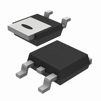
MOSFET N-CH 25V 75A SOT428
Manufacturer
NXP Semiconductors
Series
TrenchMOS™r
Datasheet
1.PSMN005-25D118.pdf
(12 pages)
Specifications of PSMN005-25D,118
Fet Type
MOSFET N-Channel, Metal Oxide
Fet Feature
Logic Level Gate
Rds On (max) @ Id, Vgs
5.8 mOhm @ 25A, 10V
Drain To Source Voltage (vdss)
25V
Current - Continuous Drain (id) @ 25° C
75A
Vgs(th) (max) @ Id
2V @ 1mA
Gate Charge (qg) @ Vgs
60nC @ 5V
Input Capacitance (ciss) @ Vds
3500pF @ 20V
Power - Max
125W
Mounting Type
Surface Mount
Package / Case
DPak, TO-252 (2 leads+tab), SC-63
Configuration
Single Dual Drain
Transistor Polarity
N-Channel
Resistance Drain-source Rds (on)
0.0058 Ohms
Drain-source Breakdown Voltage
25 V
Gate-source Breakdown Voltage
+/- 15 V
Continuous Drain Current
75 A
Power Dissipation
125 W
Maximum Operating Temperature
+ 175 C
Mounting Style
SMD/SMT
Minimum Operating Temperature
- 55 C
Lead Free Status / RoHS Status
Lead free / RoHS Compliant
Other names
934055816118
PSMN005-25D /T3
PSMN005-25D /T3
PSMN005-25D /T3
PSMN005-25D /T3


Philips Semiconductors
October 1999
N-channel logic level TrenchMOS
Fig.13. Typical turn-on gate-charge characteristics.
15
14
13
12
11
10
50
45
40
35
30
25
20
15
10
9
8
7
6
5
4
3
2
1
0
5
0
I
F
0
0
Gate-source voltage, VGS (V)
Source-Drain Diode Current, IF (A)
= f(V
ID = 75 A
VDD = 15 V
Tj = 25 C
VGS = 0 V
Fig.14. Typical reverse diode current.
0.1
10
SDS
0.2
20
); conditions: V
0.3
30
Source-Drain Voltage, VSDS (V)
0.4
Gate charge, QG (nC)
40
V
175 C
GS
0.5
50
= f(Q
0.6
GS
60
G
0.7
= 0 V; parameter T
)
70
0.8
Tj = 25 C
80
0.9
90
1
100
1.1
110
1.2
j
(TM)
7
transistor
avalanche current (I
100
10
1
0.001
Fig.15. Maximum permissible non-repetitive
Maximum Avalanche Current, I
unclamped inductive load
0.01
Tj prior to avalanche = 150 C
Avalanche time, t
AS
) versus avalanche time (t
0.1
AS
(A)
PSMN005-25D
AV
(ms)
Product specification
1
25 C
Rev 1.100
10
AV
);
Related parts for PSMN005-25D,118
Image
Part Number
Description
Manufacturer
Datasheet
Request
R

Part Number:
Description:
MOSFET N-CH 75V 75A D2PAK
Manufacturer:
NXP Semiconductors
Datasheet:
Part Number:
Description:
MOSFET N-CH 55V 75A SOT404
Manufacturer:
NXP Semiconductors
Datasheet:

Part Number:
Description:
SiliconMAX standard level N-channel enhancement mode Field-Effect Transistor (FET) in a plastic package using TrenchMOS technology
Manufacturer:
NXP Semiconductors
Datasheet:

Part Number:
Description:
MOSFET N-CH 30V 20A SOT96-1
Manufacturer:
NXP Semiconductors
Datasheet:

Part Number:
Description:
SiliconMAX logic level N-channel enhancement mode Field-Effect Transistor (FET) in a plastic package using TrenchMOS technology
Manufacturer:
NXP Semiconductors
Datasheet:

Part Number:
Description:
N-channel Logic Level Field-effect Power Transistor In A Plastic Package Using Trenchmos Technology.
Manufacturer:
NXP Semiconductors
Datasheet:
Part Number:
Description:
Psmn005-25d N-channel Logic Level Trenchmos Tm Transistor
Manufacturer:
NXP Semiconductors
Datasheet:
Part Number:
Description:
Psmn005-30k Trenchmos Tm Logic Level Fet
Manufacturer:
NXP Semiconductors
Datasheet:

Part Number:
Description:
MOSFET N-CH 55V 75A SOT78
Manufacturer:
NXP Semiconductors
Datasheet:
Part Number:
Description:
MOSFET N-CH 75V 75A TO220AB
Manufacturer:
NXP Semiconductors
Datasheet:
Part Number:
Description:
MOSFET TAPE13 PWR-MOS
Manufacturer:
NXP Semiconductors
Datasheet:

Part Number:
Description:
N-channel logic level TrenchMOS transistor
Manufacturer:
PHILIPS [NXP Semiconductors]
Datasheet:
Part Number:
Description:
NXP Semiconductors designed the LPC2420/2460 microcontroller around a 16-bit/32-bitARM7TDMI-S CPU core with real-time debug interfaces that include both JTAG andembedded trace
Manufacturer:
NXP Semiconductors
Datasheet: