IRL520NS International Rectifier, IRL520NS Datasheet - Page 2
IRL520NS
Manufacturer Part Number
IRL520NS
Description
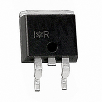
MOSFET N-CH 100V 10A D2PAK
Manufacturer
International Rectifier
Series
HEXFET®r
Datasheet
1.IRL520NS.pdf
(11 pages)
Specifications of IRL520NS
Fet Type
MOSFET N-Channel, Metal Oxide
Fet Feature
Logic Level Gate
Rds On (max) @ Id, Vgs
180 mOhm @ 6A, 10V
Drain To Source Voltage (vdss)
100V
Current - Continuous Drain (id) @ 25° C
10A
Vgs(th) (max) @ Id
2V @ 250µA
Gate Charge (qg) @ Vgs
20nC @ 5V
Input Capacitance (ciss) @ Vds
440pF @ 25V
Power - Max
3.8W
Mounting Type
Surface Mount
Package / Case
D²Pak, TO-263 (2 leads + tab)
Lead Free Status / RoHS Status
Contains lead / RoHS non-compliant
Other names
*IRL520NS
Available stocks
Company
Part Number
Manufacturer
Quantity
Price
Company:

Part Number:
IRL520NS
Manufacturer:
IR
Quantity:
12 500
Company:
Part Number:
IRL520NSPBF
Manufacturer:
IR
Quantity:
12 500
Company:
Part Number:
IRL520NSTRLPBF
Manufacturer:
SSC
Quantity:
342


Electrical Characteristics @ T
** When mounted on 1" square PCB ( FR-4 or G-10 Material ).
IRL520NS/L
Source-Drain Ratings and Characteristics
Notes:
I
I
I
V
t
Q
t
V
R
V
g
I
Q
Q
Q
t
t
t
t
C
C
C
L
DSS
S
GSS
on
d(on)
d(off)
f
SM
rr
r
For recommended footprint and soldering techniques refer to application note #AN-994.
V
fs
S
(BR)DSS
DS(on)
GS(th)
oss
SD
g
gs
gd
iss
rss
rr
max. junction temperature. ( See fig. 11 )
Repetitive rating; pulse width limited by
V
T
R
I
(BR)DSS
SD
J
DD
G
= 25 , I
= 25V, starting T
175°C
6.0A, di/dt
/ T
J
Drain-to-Source Leakage Current
Drain-to-Source Breakdown Voltage
Breakdown Voltage Temp. Coefficient
Static Drain-to-Source On-Resistance
Gate Threshold Voltage
Forward Transconductance
Gate-to-Source Forward Leakage
Gate-to-Source Reverse Leakage
Total Gate Charge
Gate-to-Source Charge
Gate-to-Drain ("Miller") Charge
Turn-On Delay Time
Rise Time
Turn-Off Delay Time
Fall Time
Input Capacitance
Output Capacitance
Reverse Transfer Capacitance
Continuous Source Current
(Body Diode)
Pulsed Source Current
(Body Diode)
Diode Forward Voltage
Reverse Recovery Time
Reverse Recovery Charge
Forward Turn-On Time
Internal Source Inductance
AS
= 6.0A. (See Figure 12)
340A/µs, V
J
= 25°C, L = 4.7mH
Parameter
Parameter
DD
V
(BR)DSS
J
= 25°C (unless otherwise specified)
,
–––
Min. Typ. Max. Units
Min. Typ. Max. Units
100
–––
–––
–––
–––
–––
–––
–––
–––
–––
–––
–––
–––
–––
–––
–––
–––
–––
–––
1.0
3.1
–––
–––
–––
–––
–––
Pulse width
Uses IRL520N data and test conditions
Intrinsic turn-on time is negligible (turn-on is dominated by L
0.11 –––
–––
–––
–––
–––
110
410
–––
––– 0.18
––– 0.22
––– 0.26
–––
–––
–––
–––
––– -100
–––
–––
–––
440
7.5
4.0
35
23
22
97
50
100
–––
160
620
–––
–––
250
–––
–––
–––
–––
–––
–––
–––
1.3
2.0
4.6
35
25
20
10
10
300µs; duty cycle
V/°C
nC
nA
nC
ns
nH
pF
A
ns
V
V
V
A
S
V
V
R
V
ƒ = 1.0MHz, See Fig. 5
MOSFET symbol
showing the
p-n junction diode.
T
T
di/dt = 100A/µs
V
Reference to 25°C, I
V
V
V
V
V
V
V
V
I
V
V
I
R
Between lead,
and center of die contact
V
integral reverse
D
D
J
J
GS
GS
GS
GS
DS
DS
DS
DS
GS
GS
DS
GS
DD
GS
DS
G
D
= 6.0A
= 6.0A
= 25°C, I
= 25°C, I
= 8.2
= 11
= 0V, I
= 10V, I
= 5.0V, I
= 4.0V, I
= V
= 25V, I
= 100V, V
= 80V, V
= 80V
= 5.0V, See Fig. 6 and 13
= 25V
= 16V
= -16V
= 50V
= 0V
GS
2%.
, I
V
D
See Fig. 10
S
F
GS
D
D
D
= 6.0A
D
D
= 250µA
GS
= 6.0A, V
Conditions
Conditions
= 250µA
= 6.0A
= 6.0A
GS
= 6.0A
= 5.0A
= 5.0V
= 0V, T
= 0V
D
= 1mA
GS
J
= 150°C
G
= 0V
S
+L
D
S
D
)
Related parts for IRL520NS
Image
Part Number
Description
Manufacturer
Datasheet
Request
R

Part Number:
Description:
SCHOTTKY RECTIFIER
Manufacturer:
International Rectifier Corp.
Datasheet:
Part Number:
Description:
SCHOTTKY RECTIFIER
Manufacturer:
International Rectifier Corp.
Datasheet:
Part Number:
Description:
SCHOTTKY RECTIFIER
Manufacturer:
International Rectifier Corp.
Datasheet:
Part Number:
Description:
SCHOTTKY RECTIFIER
Manufacturer:
International Rectifier Corp.
Datasheet:
Part Number:
Description:
SCHOTTKY RECTIFIER
Manufacturer:
International Rectifier Corp.
Datasheet:
Part Number:
Description:
SCHOTTKY RECTIFIER
Manufacturer:
International Rectifier Corp.
Datasheet:
Part Number:
Description:
SCHOTTKY RECTIFIER
Manufacturer:
International Rectifier Corp.
Datasheet:
Part Number:
Description:
SCHOTTKY RECTIFIER
Manufacturer:
International Rectifier Corp.
Datasheet:
Part Number:
Description:
SCHOTTKY RECTIFIER
Manufacturer:
International Rectifier Corp.
Datasheet:
Part Number:
Description:
SCHOTTKY RECTIFIER
Manufacturer:
International Rectifier Corp.
Datasheet:
Part Number:
Description:
SCHOTTKY RECTIFIER
Manufacturer:
International Rectifier Corp.
Datasheet:
Part Number:
Description:
SCHOTTKY RECTIFIER
Manufacturer:
International Rectifier Corp.
Datasheet:
Part Number:
Description:
SCHOTTKY RECTIFIER
Manufacturer:
International Rectifier Corp.
Datasheet:
Part Number:
Description:
SCHOTTKY RECTIFIER
Manufacturer:
International Rectifier Corp.
Datasheet:
Part Number:
Description:
SCHOTTKY RECTIFIER
Manufacturer:
International Rectifier Corp.
Datasheet: