MTW32N20E ON Semiconductor, MTW32N20E Datasheet - Page 2
MTW32N20E
Manufacturer Part Number
MTW32N20E
Description
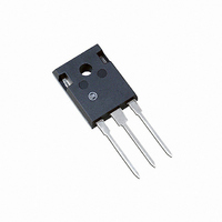
MOSFET N-CH 200V 32A TO-247
Manufacturer
ON Semiconductor
Datasheet
1.MTW32N20EG.pdf
(7 pages)
Specifications of MTW32N20E
Fet Type
MOSFET N-Channel, Metal Oxide
Fet Feature
Standard
Rds On (max) @ Id, Vgs
75 mOhm @ 16A, 10V
Drain To Source Voltage (vdss)
200V
Current - Continuous Drain (id) @ 25° C
32A
Vgs(th) (max) @ Id
4V @ 250µA
Gate Charge (qg) @ Vgs
120nC @ 10V
Input Capacitance (ciss) @ Vds
5000pF @ 25V
Power - Max
180W
Mounting Type
Through Hole
Package / Case
TO-247-3 (Straight Leads), TO-247AC
Lead Free Status / RoHS Status
Contains lead / RoHS non-compliant
Other names
MTW32N20EOS
Available stocks
Company
Part Number
Manufacturer
Quantity
Price
Company:

Part Number:
MTW32N20E
Manufacturer:
ON
Quantity:
12 500
Part Number:
MTW32N20E
Manufacturer:
MOTOROLA/摩托罗拉
Quantity:
20 000
Company:
Part Number:
MTW32N20EG
Manufacturer:
NXP
Quantity:
2 000


1. Pulse Test: Pulse Width ≤ 300 ms, Duty Cycle ≤ 2%.
2. Switching characteristics are independent of operating junction temperature.
ELECTRICAL CHARACTERISTICS
OFF CHARACTERISTICS
ON CHARACTERISTICS (Note 1)
DYNAMIC CHARACTERISTICS
SWITCHING CHARACTERISTICS (Notes 1 & 2)
SOURCE−DRAIN DIODE CHARACTERISTICS (Note 1)
INTERNAL PACKAGE INDUCTANCE
Drain−Source Breakdown Voltage
Zero Gate Voltage Drain Current
Gate−Body Leakage Current (V
Gate Threshold Voltage
Static Drain−Source On−Resistance (V
Drain−Source On−Voltage (V
Forward Transconductance (V
Input Capacitance
Output Capacitance
Reverse Transfer Capacitance
Turn−On Delay Time
Rise Time
Turn−Off Delay Time
Fall Time
Gate Charge
Forward On−Voltage
Reverse Recovery Time
Reverse Recovery Stored Charge
Internal Drain Inductance
Internal Source Inductance
(V
Temperature Coefficient (Positive)
(V
(V
(V
Temperature Coefficient (Negative)
(I
(I
(Measured from the drain lead 0.25″ from package to center of die)
(Measured from the source lead 0.25″ from package to source bond pad)
D
D
GS
DS
DS
DS
= 32 Adc)
= 16 Adc, T
= 0 V, I
= 200 Vdc, V
= 200 Vdc, V
= V
GS
, I
D
D
= 250 mAdc)
J
= 250 mAdc)
= 125°C)
GS
GS
= 0)
= 0, T
GS
DS
J
GS
= 125°C)
= 10 Vdc)
= 15 Vdc, I
= ± 20 Vdc, V
Characteristic
GS
(T
(I
= 10 Vdc, I
S
(V
J
D
(I
= 32 Adc, V
= 25°C unless otherwise noted)
DS
S
= 16 Adc)
(V
(V
= 16 Adc, V
DS
V
= 25 Vdc, V
DD
DS
GS
(I
= 0)
S
= 100 Vdc, I
= 160 Vdc, I
D
= 10 Vdc, R
= 32 Adc, V
V
= 16 Adc)
GS
GS
http://onsemi.com
= 10 Vdc)
GS
= 0, dI
GS
= 0, T
= 0, f = 1.0 MHz)
D
D
G
GS
S
= 32 Adc,
= 32 Adc,
= 6.2 W)
/dt = 100 A/ms)
2
J
= 0)
= 125°C)
V
Symbol
R
V
V
(BR)DSS
t
t
I
I
C
Q
DS(on)
DS(on)
C
V
GS(th)
C
d(on)
g
d(off)
DSS
GSS
Q
Q
Q
Q
L
L
t
t
t
FS
oss
t
t
SD
rss
RR
iss
rr
a
b
r
D
S
f
T
1
2
3
Min
200
2.0
12
−
−
−
−
−
−
−
−
−
−
−
−
−
−
−
−
−
−
−
−
−
−
−
−
−
−
−
0.064
3600
2.94
Typ
247
130
690
120
280
195
8.0
1.1
0.9
5.0
25
75
91
85
12
40
30
85
13
−
−
−
−
−
−
−
−
0.075
1000
5000
1000
Max
250
100
250
240
150
182
120
4.0
3.0
2.7
2.0
50
−
−
−
−
−
−
−
−
−
−
−
−
−
−
mV/°C
mV/°C
mhos
mAdc
nAdc
Unit
Vdc
Vdc
Vdc
Vdc
nC
mC
nH
nH
pF
ns
ns
W
Related parts for MTW32N20E
Image
Part Number
Description
Manufacturer
Datasheet
Request
R

Part Number:
Description:
ON Semiconductor [VOLTAGE REGULATOR]
Manufacturer:
ON Semiconductor
Datasheet:
Part Number:
Description:
357-036-542-201 CARDEDGE 36POS DL .156 BLK LOPRO
Manufacturer:
ON Semiconductor
Datasheet:
Part Number:
Description:
357-036-542-201 CARDEDGE 36POS DL .156 BLK LOPRO
Manufacturer:
ON Semiconductor
Datasheet:
Part Number:
Description:
357-036-542-201 CARDEDGE 36POS DL .156 BLK LOPRO
Manufacturer:
ON Semiconductor
Datasheet:
Part Number:
Description:
357-036-542-201 CARDEDGE 36POS DL .156 BLK LOPRO
Manufacturer:
ON Semiconductor
Datasheet:
Part Number:
Description:
357-036-542-201 CARDEDGE 36POS DL .156 BLK LOPRO
Manufacturer:
ON Semiconductor
Datasheet:
Part Number:
Description:
357-036-542-201 CARDEDGE 36POS DL .156 BLK LOPRO
Manufacturer:
ON Semiconductor
Datasheet:
Part Number:
Description:
357-036-542-201 CARDEDGE 36POS DL .156 BLK LOPRO
Manufacturer:
ON Semiconductor
Datasheet:
Part Number:
Description:
357-036-542-201 CARDEDGE 36POS DL .156 BLK LOPRO
Manufacturer:
ON Semiconductor
Datasheet:
Part Number:
Description:
357-036-542-201 CARDEDGE 36POS DL .156 BLK LOPRO
Manufacturer:
ON Semiconductor
Datasheet:
Part Number:
Description:
357-036-542-201 CARDEDGE 36POS DL .156 BLK LOPRO
Manufacturer:
ON Semiconductor
Datasheet:
Part Number:
Description:
Manufacturer:
ON Semiconductor
Datasheet:
Part Number:
Description:
Manufacturer:
ON Semiconductor
Datasheet:
Part Number:
Description:
Manufacturer:
ON Semiconductor
Datasheet: