NTP2955 ON Semiconductor, NTP2955 Datasheet

MOSFET P-CH 60V 2.4A TO220AB

NTP2955

Manufacturer Part Number
NTP2955
Description
MOSFET P-CH 60V 2.4A TO220AB
Manufacturer
ON Semiconductor
Datasheet

Specifications of NTP2955

Fet Type
MOSFET P-Channel, Metal Oxide
Fet Feature
Standard
Rds On (max) @ Id, Vgs
196 mOhm @ 12A, 10V
Drain To Source Voltage (vdss)
60V
Current - Continuous Drain (id) @ 25° C
2.4A
Vgs(th) (max) @ Id
4V @ 250µA
Gate Charge (qg) @ Vgs
14nC @ 10V
Input Capacitance (ciss) @ Vds
700pF @ 25V
Power - Max
2.4W
Mounting Type
Through Hole
Package / Case
TO-220-3 (Straight Leads)
Configuration
Single
Transistor Polarity
P-Channel
Resistance Drain-source Rds (on)
0.156 Ohms
Forward Transconductance Gfs (max / Min)
6 S
Drain-source Breakdown Voltage
- 60 V
Gate-source Breakdown Voltage
+/- 20 V
Continuous Drain Current
- 12 A
Power Dissipation
2.4 W
Maximum Operating Temperature
+ 175 C
Mounting Style
Through Hole
Minimum Operating Temperature
- 55 C
Lead Free Status / RoHS Status
Contains lead / RoHS non-compliant

Available stocks

Company
Part Number
Manufacturer
Quantity
Price
Part Number:
NTP2955G
Manufacturer:
ON
Quantity:
9 520
Part Number:
NTP2955G
Manufacturer:
JRC
Quantity:
10 000
Part Number:
NTP2955G
Manufacturer:
ON/安森美
Quantity:
20 000
NTP2955
Power MOSFET
−60 V, −12 A, Single P−Channel, TO−220
Features
Applications
Stresses exceeding Maximum Ratings may damage the device. Maximum
Ratings are stress ratings only. Functional operation above the Recommended
Operating Conditions is not implied. Extended exposure to stresses above the
Recommended Operating Conditions may affect device reliability.
1. When surface mounted to an FR4 board using 1 in pad size
*For additional information on our Pb−Free strategy and soldering details, please
MAXIMUM RATINGS
© Semiconductor Components Industries, LLC, 2006
March, 2006 − Rev. 2
THERMAL RESISTANCE RATINGS
download the ON Semiconductor Soldering and Mounting Techniques
Reference Manual, SOLDERRM/D.
Drain−to−Source Voltage
Gate−to−Source Voltage
Continuous Drain
Power Dissipation
Continuous Drain
Power Dissipation
Pulsed Drain Current
Operating Junction and Storage Temperature
Source Current (Body Diode)
Single Pulse Drain−to−Source Avalanche
Lead Temperature for Soldering Purposes
Junction−to−Case
Junction−to−Ambient − Steady State (Note 1)
Low R
Rugged Performance
Fast Switching
Pb−Free Package is Available*
Industrial
Automotive
Power Supplies
(Cu. area = 1.127 in sq [1 oz] including traces).
Current (Note 1)
(Note 1)
Current (Note 1)
(Note 1)
Energy (V
I
(1/8” from case for 10 s)
PK
= −12 A, L = 3.0 mH, R
DS(on)
DD
= −30 V, V
Parameter
Parameter
(T
J
Steady
Steady
G
= 25°C unless otherwise noted)
State
State
= −10 V,
G
= 3.0 W)
t
p
= 10 ms
T
T
T
T
T
T
A
A
A
C
C
C
= 25°C
= 85°C
= 25°C
= 25°C
= 85°C
= 25°C
Symbol
Symbol
V
T
EAS
V
R
R
I
P
P
T
DSS
STG
T
I
I
DM
I
GS
D
D
S
qJC
qJA
J
D
D
L
,
−55 to
Value
−9.0
62.5
−2.4
−1.8
Max
62.5
−60
±20
−12
−42
175
−12
216
260
2.4
2.4
1
°C/W
Unit
Unit
mJ
°C
°C
W
W
V
V
A
A
A
A
NTP2955
NTP2955G
V
−60 V
(BR)DSS
CASE 221A
Device
STYLE 5
TO−220
1
2
ORDERING INFORMATION
3
A
Y
WW
G
G
http://onsemi.com
156 mW @ −10 V
(Pb−Free)
R
Package
= Assembly Location
= Year
= Work Week
= Pb−Free Package
TO−220
TO−220
P−Channel
DS(on)
D
Publication Order Number:
MARKING DIAGRAM &
Typ
PIN ASSIGNMENT
S
50 Units / Rail
50 Units / Rail
1
NT2955G
G
Shipping
AYWW
NTP2955/D
D
D S
I
D
−12 A
MAX

Related parts for NTP2955

NTP2955 Summary of contents

Page 1

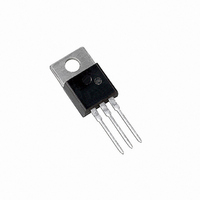
... NTP2955G 1 http://onsemi.com R Typ I MAX DS(on) D 156 mW @ −10 V −12 A P−Channel MARKING DIAGRAM & PIN ASSIGNMENT D NT2955G AYWW Assembly Location Y = Year WW = Work Week G = Pb−Free Package ORDERING INFORMATION Package Shipping TO−220 50 Units / Rail TO−220 50 Units / Rail (Pb−Free) Publication Order Number: NTP2955/D ...

Page 2

ELECTRICAL CHARACTERISTICS Parameter OFF CHARACTERISTICS Drain−to−Source Breakdown Voltage Drain−to−Source Breakdown Voltage Temperature Coefficient Zero Gate Voltage Drain Current Gate−to−Source Leakage Current ON CHARACTERISTICS (Note 2) Gate Threshold Voltage Negative Threshold Temperature Coefficient Drain−to−Source On Resistance Forward Transconductance CHARGES AND CAPACITANCES ...

Page 3

T = 25°C J −8 − −7.0 V −9 −6 −5 −5 −4.0 V −4 −V , DRAIN−TO−SOURCE VOLTAGE ...

Page 4

V = −0 V 1100 GS C ISS 1000 900 800 C RSS 700 600 C 500 400 300 C OSS 200 C RSS 100 V = − −10 − −V −V GS ...

Page 5

... V 0.045 −−− 1.15 −−− Z −−− 0.080 −−− 2.04 STYLE 5: PIN 1. GATE 2. DRAIN 3. SOURCE 4. DRAIN ON Semiconductor Website: http://onsemi.com Order Literature: http://www.onsemi.com/litorder For additional information, please contact your local Sales Representative. NTP2955/D ...

Related keywords