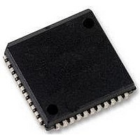
SCC68681C1A44 NXP Semiconductors, SCC68681C1A44 Datasheet - Page 12

SCC68681C1A44
Manufacturer Part Number
SCC68681C1A44
Description
UART 2-CH 5V 44-Pin PLCC Tube
Manufacturer
NXP Semiconductors
Datasheet
1.SCC68681C1A44512.pdf
(29 pages)
Specifications of SCC68681C1A44
Package
44PLCC
Number Of Channels Per Chip
2
Maximum Data Rate
0.1152 MBd
Transmitter And Receiver Fifo Counter
No
Operating Supply Voltage
5 V
Minimum Single Supply Voltage
4.5 V
Maximum Processing Temperature
260 °C
Maximum Supply Current
10 mA
No. Of Channels
2
Uart Features
Quadruple Buffered Receiver Data Register
Supply Voltage Range
4.5V To 5.5V
Operating Temperature Range
0°C To +70°C
Digital Ic Case Style
PLCC
No. Of Pins
44
Data Rate
115.2Kilobaud
Rohs Compliant
Yes
Lead Free Status / RoHS Status
Lead free / RoHS Compliant
Available stocks
Company
Part Number
Manufacturer
Quantity
Price
Company:
Part Number:
SCC68681C1A44
Manufacturer:
FREESCALE
Quantity:
1 596
Company:
Part Number:
SCC68681C1A44
Manufacturer:
PHI
Quantity:
5 530
Company:
Part Number:
SCC68681C1A44
Manufacturer:
PH
Quantity:
504
Part Number:
SCC68681C1A44
Manufacturer:
NXP/恩智浦
Quantity:
20 000
Company:
Part Number:
SCC68681C1A44,512
Manufacturer:
NXP Semiconductors
Quantity:
10 000
Company:
Part Number:
SCC68681C1A44,518
Manufacturer:
NXP Semiconductors
Quantity:
10 000
Company:
Part Number:
SCC68681C1A44,529
Manufacturer:
NXP Semiconductors
Quantity:
10 000
Company:
Part Number:
SCC68681C1A44529
Manufacturer:
NXP Semiconductors
Quantity:
135
the underrun condition, the issuing of the transmitter disable must be
lengths of 6, 7, and 8 bits. For a character lengths of 5 bits, 1-1/16 to
applied via CRB. After reading or writing MR1B, the pointer will point
The bit definitions for mode register are identical to the bit definitions
Philips Semiconductors
commands issued via the SOPR and ROPR registers. MR2[5] set to
1 caused the RTSN to be reset automatically one bit time after the
character(s) in the transmit shift register and in the THR (if any) are
completely transmitted (including the programmed number of stop
bits) if a previously issued transmitter disable is pending. This
feature can be used to automatically terminate the transmission as
follows:
1. Program the auto-reset mode: MR2[5]=1
2. Enable transmitter, if not already enabled
3. Set OPR[0] or OPR[1] to ‘1’ via SOPR and ROPR.
4. Send message
5. After the last character of the message is loaded to the THR,
6. The last character will be transmitted and the RTSN will be reset
NOTE: The transmitter is in an underrun condition when both the
TxRDY and the TxEMT bits are set. This condition also exists
immediately after the transmitter is enabled from the disabled or
reset state. When using the above procedure with the transmitter in
delayed from the loading of a single, or last, character until the
TxRDY becomes active again after the character is loaded.
MR2A[4] – Channel A Clear-to-Send Control
If this bit is 0, CTSAN has no effect on the transmitter. If this bit is a
1, the transmitter checks the state of CTSAN (IP0) each time it is
ready to send a character. If IP0 is asserted (LOW), the character is
transmitted. If it is negated (HIGH), the TxDA output remains in the
marking state and the transmission is delayed until CTSAN goes
LOW. Changes in CTSAN while a character is being transmitted do
not affect the transmission of that character.
MR2A[3:0] – Channel A Stop Bit Length Select
This field programs the length of the stop bit appended to the
transmitted character. Stop bit lengths of 9/16 to 1 and 1-9/16 to 2
bits, in increments of 1/16 bit, can be programmed for character
2 stop bits can be programmed in increments of 1/16 bit. The
receiver only checks for a ‘mark’ condition at the center of the first
stop bit position (one bit time after the last data bit, or after the parity
bit is enabled), in all cases.
If an external 1 clock is used for the transmitter, MR2A[3] = 0
selects one stop bit and MR2A[3] = 1 selects two stop bits to be
transmitted.
MR1B – Channel B Mode Register 1
MR1B is accessed when the Channel B MR pointer points to MR1.
The pointer is set to MR1 by RESET or by a ‘set pointer’ command
to MR2B.
The bit definitions for this register are identical to MR1A, except that
all control actions apply to the Channel B receiver and transmitter
and the corresponding inputs and outputs.
MR2B – Channel B Mode Register 2
MR2B is accessed when the Channel B MR pointer points to MR2,
which occurs after any access to MR1B. Accesses to MR2B do not
change the pointer.
for MR2A, except that all control actions apply to the Channel B
receiver and transmitter and the corresponding inputs and outputs.
2004 Apr 06
Dual asynchronous receiver/transmitter (DUART)
disable the transmitter. (If the transmitter is underrun, a special
case exists. See note below.)
one bit time after the last stop bit is sent.
12
This field selects the baud rate clock for the Channel A receiver. The
CSRA – Channel A Clock Select Register
CSRA[7:4] – Channel A Receiver Clock Select
field definition is shown in Table 3.
CSRA[3:0] – Channel A Transmitter Clock Select
This field selects the baud rate clock for the Channel A transmitter.
The field definition is as shown in Table 3, except as follows:
The transmitter and receiver clock is always a 16 clock except
for 1111 selection.
Table 3. X1 clock = 3.6864 MHz
See Table 6 for other rates to 115.2 k baud.
CSRA[3:0]
CSRA[7:4]
0000
0001
0010
0011
0100
0101
0110
1000
1001
1010
1011
1100
1101
1110
1111
0111
1110
1111
IP4–16
IP4–1
IP3–16
IP3–1
Timer
ACR[7] = 0
ACR[7] = 0
1,200
1,050
2,400
4,800
7,200
9,600
134.5
200
300
600
110
50
38.4 k
Baud Rate
Baud Rate
SCC68681
IP4–16
IP3–16
IP3–1
IP4–1
ACR[7] = 1
ACR[7] = 1
1,200
2,000
2,400
4,800
1,800
9,600
Timer
134.5
150
300
600
110
75
19.2 k
Product data


