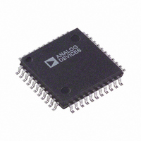
AD6600ASTZ Analog Devices Inc, AD6600ASTZ Datasheet - Page 2
AD6600ASTZ
Manufacturer Part Number
AD6600ASTZ
Description
ADC Single 20MSPS 11-Bit Parallel 44-Pin LQFP
Manufacturer
Analog Devices Inc
Datasheet
1.AD6600ASTZ-REEL.pdf
(24 pages)
Specifications of AD6600ASTZ
Package
44LQFP
Resolution
11 Bit
Sampling Rate
20000 KSPS
Number Of Adcs
1
Number Of Analog Inputs
2
Digital Interface Type
Parallel
Input Type
Voltage
Signal To Noise Ratio
59(Typ) dB
Sample And Hold
Yes
Polarity Of Input Voltage
Bipolar
Number Of Bits
11
Sampling Rate (per Second)
20M
Data Interface
Parallel
Number Of Converters
1
Power Dissipation (max)
976mW
Voltage Supply Source
Single Supply
Operating Temperature
-40°C ~ 85°C
Mounting Type
Surface Mount
Package / Case
44-LQFP
Lead Free Status / RoHS Status
Lead free / RoHS Compliant
Available stocks
Company
Part Number
Manufacturer
Quantity
Price
Company:

Part Number:
AD6600ASTZ
Manufacturer:
Analog Devices Inc
Quantity:
10 000
Part Number:
AD6600ASTZ
Manufacturer:
ADI/亚德诺
Quantity:
20 000
Company:
Part Number:
AD6600ASTZ-REEL
Manufacturer:
Analog Devices Inc
Quantity:
10 000


AD6600–SPECIFICATIONS
DC SPECIFICATIONS
Parameter
ANALOG INPUTS (AIN, AIN/BIN, BIN)
PEAK DETECTOR (Internal), RSSI
RESONANT PORT (FLT, FLT)
A/D CONVERTER
ENCODE INPUTS (ENC, ENC)
A/B MODE INPUTS (A_SEL, B_SEL)
POWER SUPPLY
POWER CONSUMPTION
NOTES
1
2
3
4
5
6
Specifications subject to change without notice.
DIGITAL SPECIFICATIONS
Parameter
LOGIC OUTPUTS (D10–D0, AB_OUT, RSSI2–0)
CLK2× OUTPUT
NOTES
1
2
Specifications subject to change without notice.
Analog Input Range is a function of input frequency. See ac specifications for 70 MHz–250 MHz inputs.
Analog Input Impedance is a function of input frequency. See ac specifications for 70 MHz–450 MHz inputs.
Six dB of digital hysteresis is used to eliminate level uncertainty at the RSSI threshold points due to noise and amplitude variations.
Encode inputs should be ac-coupled and driven differentially. See Encoding the AD6600 for details.
A_SEL and B_SEL should be tied directly to ground or AVCC.
Maximum power consumption is computed as maximum current at nominal supplies.
Digital output load is one LCX gate.
CLK2× output voltage levels, high and low, tested at switching rate of 10 MHz.
Differential Analog Input Voltage Range
Differential Analog Input Resistance
Differential Analog Input Capacitance
Resolution
RSSI Gain Step
RSSI Hysteresis
Differential Port Resistance
Differential Port Capacitance
Resolution
Differential Input Voltage (AC-Coupled)
Differential Input Resistance
Differential Input Capacitance
Input High Voltage Range
Input Low Voltage Range
Supply Voltages
Supply Current
Logic Compatibility
Logic “1” Voltage (DVCC = 3.3 V)
Logic “0” Voltage (DVCC = 3.3 V)
Logic “1” Voltage (DVCC = 5.0 V)
Logic “0” Voltage (DVCC = 5.0 V)
Output Coding (D10–D0)
Logic “1” Voltage (DVCC = 3.3 V)
Logic “0” Voltage (DVCC = 3.3 V)
Logic “1” Voltage (DVCC = 5.0 V)
Logic “0” Voltage (DVCC = 5.0 V)
AVCC
DVCC
I
I
AVCC
DVCC
(AVCC = 5.0 V)
(DVCC = 3.3 V)
3
1, 2
6
(AVCC = 5 V, DVCC = 3.3 V; T
2
(AVCC = 5 V, DVCC = 3.3 V; T
5
1
4
Temp
Full
Full
25°C
Full
Full
Full
Full
Full
Full
25°C
25°C
Full
Full
Full
Full
Full
Full
Full
Temp
Full
Full
Full
Full
Full
Full
Full
Full
1
MIN
= –40 C, T
Test
Level
V
IV
V
V
V
V
V
IV
IV
V
V
IV
IV
II
IV
II
II
II
Test
Level
II
II
IV
IV
II
II
IV
IV
MIN
= –40 C, T
MAX
= +85 C unless otherwise noted.)
MAX
Min
160
0.4
4.75
0.0
4.75
3.0
Min
2.8
4.0
2.8
4.0
= +85 C unless otherwise noted.)
AD6600AST
AD6600AST
Two’s Complement
Typ
2.0
200
1.5
3
6
6
11
11
2.5
5.0
3.3
145
15
775
Typ
DVCC – 0.2
DVCC – 0.35
0.35
DVCC – 0.2
0.2
DVCC – 0.3
0.35
630
1.75
CMOS
0.2
Max
240
5.25
0.5
5.25
5.25
182
20
976
Max
0.5
0.5
0.5
0.5
Unit
V p-p
Ω
pF
Bits
dB
dB
Ω
pF
Bits
V p-p
kΩ
pF
V
V
V
mA
mA
mW
Unit
V
V
V
V
V
V
V
V
V
Related parts for AD6600ASTZ
Image
Part Number
Description
Manufacturer
Datasheet
Request
R

Part Number:
Description:
±1.7g Dual-Axis IMEMS Accelerometer Evaluation Board
Manufacturer:
Analog Devices Inc
Datasheet:

Part Number:
Description:
Inertial Sensor Evaluation System
Manufacturer:
Analog Devices Inc
Datasheet:
Part Number:
Description:
Manufacturer:
Analog Devices Inc
Datasheet:
Part Number:
Description:
Manufacturer:
Analog Devices Inc
Datasheet:
Part Number:
Description:
Manufacturer:
Analog Devices Inc
Datasheet:
Part Number:
Description:
Manufacturer:
Analog Devices Inc
Datasheet:
Part Number:
Description:
Manufacturer:
Analog Devices Inc
Datasheet:
Part Number:
Description:
Manufacturer:
Analog Devices Inc
Datasheet:
Part Number:
Description:
Manufacturer:
Analog Devices Inc
Datasheet:
Part Number:
Description:
Manufacturer:
Analog Devices Inc
Datasheet:
Part Number:
Description:
Manufacturer:
Analog Devices Inc
Datasheet:
Part Number:
Description:
Manufacturer:
Analog Devices Inc
Datasheet:
Part Number:
Description:
Manufacturer:
Analog Devices Inc
Datasheet: