BLF175,112 NXP Semiconductors, BLF175,112 Datasheet - Page 2
BLF175,112
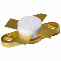
Manufacturer Part Number
BLF175,112
Description
TRANSISTOR RF DMOS SOT123A
Manufacturer
NXP Semiconductors
Datasheet
1.BLF175112.pdf
(21 pages)
Specifications of BLF175,112
Package / Case
SOT-123A
Transistor Type
N-Channel
Frequency
108MHz
Gain
20dB
Voltage - Rated
125V
Current Rating
4A
Current - Test
30mA
Voltage - Test
50V
Power - Output
30W
Minimum Operating Temperature
- 65 C
Mounting Style
SMD/SMT
Resistance Drain-source Rds (on)
1.5 Ohm @ 10 V
Transistor Polarity
N-Channel
Configuration
Single Dual Source
Drain-source Breakdown Voltage
125 V
Gate-source Breakdown Voltage
+/- 20 V
Continuous Drain Current
4 A
Power Dissipation
68000 mW
Maximum Operating Temperature
+ 200 C
Application
HF/VHF
Channel Type
N
Channel Mode
Enhancement
Drain Source Voltage (max)
125V
Output Power (max)
30W
Power Gain (typ)@vds
44@50V/24@50V/20@50VdB
Frequency (max)
108MHz
Package Type
SOT-123A
Pin Count
4
Forward Transconductance (typ)
1.6S
Drain Source Resistance (max)
1500@10Vmohm
Input Capacitance (typ)@vds
130@50VpF
Output Capacitance (typ)@vds
36@50VpF
Reverse Capacitance (typ)
3.7@50VpF
Operating Temp Range
-65C to 200C
Drain Efficiency (typ)
65%
Mounting
Screw
Mode Of Operation
CW Class B/Class-A/Class-AB
Number Of Elements
1
Power Dissipation (max)
68000mW
Vswr (max)
50
Screening Level
Military
Lead Free Status / RoHS Status
Lead free / RoHS Compliant
Noise Figure
-
Lead Free Status / Rohs Status
Lead free / RoHS Compliant
Other names
568-2400
933939780112
BLF175
BLF175
933939780112
BLF175
BLF175


Philips Semiconductors
FEATURES
DESCRIPTION
Silicon N-channel enhancement
mode vertical D-MOS transistor
designed for large signal amplifier
applications in the HF/VHF frequency
range.
The transistor has a 4-lead, SOT123A
flange package, with a ceramic cap.
All leads are isolated from the flange.
A marking code, showing gate-source
voltage (V
for matched pair applications. Refer
to the handbook 'General' section for
further information.
PINNING - SOT123A
QUICK REFERENCE DATA
RF performance at T
Note
1. 2-tone efficiency.
2003 Jul 22
class-A
class-AB
CW, class-B
High power gain
Low intermodulation distortion
Easy power control
Good thermal stability
Withstands full load mismatch
Gold metallization ensures
excellent reliability.
HF/VHF power MOS transistor
PIN
1
2
3
4
OPERATION
MODE OF
drain
source
gate
source
GS
) information is provided
DESCRIPTION
h
= 25 C in a common source test circuit.
(MH
108
28
28
f
Z
)
ook, halfpage
PIN CONFIGURATION
This product is supplied in anti-static packing to prevent damage caused by
electrostatic discharge during transport and handling. For further information,
refer to Philips specs.: SNW-EQ-608, SNW-FQ-302A, and SNW-FQ-302B.
Product and environmental safety - toxic materials
This product contains beryllium oxide. The product is entirely safe provided
that the BeO disc is not damaged. All persons who handle, use or dispose of
this product should be aware of its nature and of the necessary safety
precautions. After use, dispose of as chemical or special waste according to
the regulations applying at the location of the user. It must never be thrown
out with the general or domestic waste.
V
(V)
50
50
50
DS
1
2
(mA)
800
150
I
30
DQ
2
Fig.1 Simplified outline and symbol.
30 (PEP)
8 (PEP)
(W)
P
30
MSB057
L
4
3
WARNING
CAUTION
typ. 24
typ. 20
(dB)
G
24
p
typ. 40
typ. 65
Product specification
(%)
D
(1)
g
MBB072
BLF175
typ. 35
d
s
(dB)
d
40
3
Related parts for BLF175,112
Image
Part Number
Description
Manufacturer
Datasheet
Request
R

Part Number:
Description:
Description: Silicon N-channel enhancement mode vertical D-MOS transistor designed for large signal amplifier applications in the HF/VHF frequency range
Manufacturer:
NXP Semiconductors
Datasheet:

Part Number:
Description:
NXP Semiconductors designed the LPC2420/2460 microcontroller around a 16-bit/32-bitARM7TDMI-S CPU core with real-time debug interfaces that include both JTAG andembedded trace
Manufacturer:
NXP Semiconductors
Datasheet:

Part Number:
Description:
NXP Semiconductors designed the LPC2458 microcontroller around a 16-bit/32-bitARM7TDMI-S CPU core with real-time debug interfaces that include both JTAG andembedded trace
Manufacturer:
NXP Semiconductors
Datasheet:
Part Number:
Description:
NXP Semiconductors designed the LPC2468 microcontroller around a 16-bit/32-bitARM7TDMI-S CPU core with real-time debug interfaces that include both JTAG andembedded trace
Manufacturer:
NXP Semiconductors
Datasheet:
Part Number:
Description:
NXP Semiconductors designed the LPC2470 microcontroller, powered by theARM7TDMI-S core, to be a highly integrated microcontroller for a wide range ofapplications that require advanced communications and high quality graphic displays
Manufacturer:
NXP Semiconductors
Datasheet:
Part Number:
Description:
NXP Semiconductors designed the LPC2478 microcontroller, powered by theARM7TDMI-S core, to be a highly integrated microcontroller for a wide range ofapplications that require advanced communications and high quality graphic displays
Manufacturer:
NXP Semiconductors
Datasheet:
Part Number:
Description:
The Philips Semiconductors XA (eXtended Architecture) family of 16-bit single-chip microcontrollers is powerful enough to easily handle the requirements of high performance embedded applications, yet inexpensive enough to compete in the market for hi
Manufacturer:
NXP Semiconductors
Datasheet:
Part Number:
Description:
The XA-S3 device is a member of Philips Semiconductors? XA(eXtended Architecture) family of high performance 16-bitsingle-chip microcontrollers
Manufacturer:
NXP Semiconductors
Datasheet:

Part Number:
Description:
The NXP BlueStreak LH75401/LH75411 family consists of two low-cost 16/32-bit System-on-Chip (SoC) devices
Manufacturer:
NXP Semiconductors
Datasheet:
Part Number:
Description:
The NXP LPC3130/3131 combine an 180 MHz ARM926EJ-S CPU core, high-speed USB2
Manufacturer:
NXP Semiconductors
Datasheet:
Part Number:
Description:
The NXP LPC3141 combine a 270 MHz ARM926EJ-S CPU core, High-speed USB 2
Manufacturer:
NXP Semiconductors
Part Number:
Description:
The NXP LPC3143 combine a 270 MHz ARM926EJ-S CPU core, High-speed USB 2
Manufacturer:
NXP Semiconductors

Part Number:
Description:
The NXP LPC3152 combines an 180 MHz ARM926EJ-S CPU core, High-speed USB 2
Manufacturer:
NXP Semiconductors
Part Number:
Description:
The NXP LPC3154 combines an 180 MHz ARM926EJ-S CPU core, High-speed USB 2
Manufacturer:
NXP Semiconductors