BLL1214-250,112 NXP Semiconductors, BLL1214-250,112 Datasheet - Page 2
BLL1214-250,112
Manufacturer Part Number
BLL1214-250,112
Description
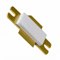
TRANSISTOR RF LDMOS SOT502A
Manufacturer
NXP Semiconductors
Datasheet
1.BLL1214-250112.pdf
(10 pages)
Specifications of BLL1214-250,112
Package / Case
SOT502A
Transistor Type
LDMOS
Frequency
1.2GHz ~ 1.4GHz
Gain
12dB
Voltage - Rated
75V
Current Rating
45A
Current - Test
150mA
Voltage - Test
36V
Power - Output
250W
Minimum Operating Temperature
- 65 C
Mounting Style
SMD/SMT
Product Type
RF MOSFET Power
Resistance Drain-source Rds (on)
0.06 Ohms
Transistor Polarity
N-Channel
Configuration
Single
Drain-source Breakdown Voltage
75 V
Gate-source Breakdown Voltage
+/- 22 V
Power Dissipation
400 W
Maximum Operating Temperature
+ 200 C
Application
L-Band
Channel Type
N
Channel Mode
Enhancement
Drain Source Voltage (max)
75V
Output Power (max)
250W
Power Gain (typ)@vds
12(Min)@36VdB
Frequency (min)
1.2GHz
Frequency (max)
1.4GHz
Package Type
LDMOST
Pin Count
3
Forward Transconductance (typ)
9S
Drain Source Resistance (max)
60(Typ)@9Vmohm
Operating Temp Range
-65C to 200C
Drain Efficiency (typ)
42(Min)%
Mounting
Screw
Mode Of Operation
Pulsed RF Class-AB
Number Of Elements
1
Power Dissipation (max)
400000mW
Vswr (max)
3
Screening Level
Military
Lead Free Status / RoHS Status
Lead free / RoHS Compliant
Noise Figure
-
Lead Free Status / Rohs Status
Compliant
Other names
568-2424
934056925112
BLL1214-250
BLL1214-250
934056925112
BLL1214-250
BLL1214-250
Available stocks
Company
Part Number
Manufacturer
Quantity
Price
Company:

Part Number:
BLL1214-250,112
Manufacturer:
NXP
Quantity:
1 400


Philips Semiconductors
FEATURES
APPLICATIONS
DESCRIPTION
Silicon N-channel enhancement mode lateral D-MOS
transistor encapsulated in a 2-lead flange package
(SOT502A) with a ceramic cap. The common source is
connected to the flange.
QUICK REFERENCE DATA
RF performance at T
LIMITING VALUES
In accordance with the Absolute Maximum Rating System (IEC 60134).
2003 Aug 29
Pulsed class-AB;
t
V
V
P
T
T
This product is supplied in anti-static packing to prevent damage caused by electrostatic discharge during transport
and handling. For further information, refer to Philips specs.: SNW-EQ-608, SNW-FQ-302A and SNW-FQ-302B.
p
SYMBOL
stg
j
High power gain
Easy power control
Excellent ruggedness
Source on mounting base eliminates DC isolators,
reducing common mode inductance.
L-band radar applications in the 1200 to 1400 MHz
frequency range.
DS
GS
tot
L-band radar LDMOS transistor
= 1 ms;
OPERATION
MODE OF
= 10%
drain-source voltage
gate-source voltage
total power dissipation
storage temperature
junction temperature
h
= 25 C in a common source test circuit.
1200 to 1400
PARAMETER
(MHz)
f
V
(V)
36
DS
(mA)
T
150
I
DQ
h
CAUTION
70 C; t
2
CONDITIONS
PINNING - SOT502A
handbook, halfpage
(W)
250
P
L
p
= 1 ms; = 10%
PIN
1
2
3
(dB)
>12
G
p
Fig.1 Simplified outline.
Top view
drain
gate
source, connected to flange
>42
(%)
D
65
MIN.
1
2
droop
pulse
DESCRIPTION
(dB)
<0.6
BLL1214-250
Product specification
75
400
150
200
MBK394
22
MAX.
3
<100
(ns)
t
r
V
V
W
C
C
UNIT
<100
(ns)
t
f
Related parts for BLL1214-250,112
Image
Part Number
Description
Manufacturer
Datasheet
Request
R

Part Number:
Description:
Silicon N-channel enhancement mode lateral D-MOS transistor encapsulated in a 2-lead flange package (SOT502A) with a ceramic cap
Manufacturer:
NXP Semiconductors
Datasheet:
Part Number:
Description:
Silicon N-channel enhancement mode lateral D-MOS transistor encapsulated in a 2-lead flange package (SOT502A) with a ceramic cap
Manufacturer:
NXP Semiconductors
Datasheet:

Part Number:
Description:
RF MOSFET Power BULK TNS-MICP
Manufacturer:
NXP Semiconductors
Datasheet:

Part Number:
Description:
TRANSISTOR RF LDMOS SOT467C
Manufacturer:
NXP Semiconductors
Datasheet:

Part Number:
Description:
TRANS L-BAND RADAR LDMOS SOT502A
Manufacturer:
NXP Semiconductors
Datasheet:
Part Number:
Description:
NXP Semiconductors designed the LPC2420/2460 microcontroller around a 16-bit/32-bitARM7TDMI-S CPU core with real-time debug interfaces that include both JTAG andembedded trace
Manufacturer:
NXP Semiconductors
Datasheet:

Part Number:
Description:
NXP Semiconductors designed the LPC2458 microcontroller around a 16-bit/32-bitARM7TDMI-S CPU core with real-time debug interfaces that include both JTAG andembedded trace
Manufacturer:
NXP Semiconductors
Datasheet:
Part Number:
Description:
NXP Semiconductors designed the LPC2468 microcontroller around a 16-bit/32-bitARM7TDMI-S CPU core with real-time debug interfaces that include both JTAG andembedded trace
Manufacturer:
NXP Semiconductors
Datasheet:
Part Number:
Description:
NXP Semiconductors designed the LPC2470 microcontroller, powered by theARM7TDMI-S core, to be a highly integrated microcontroller for a wide range ofapplications that require advanced communications and high quality graphic displays
Manufacturer:
NXP Semiconductors
Datasheet:
Part Number:
Description:
NXP Semiconductors designed the LPC2478 microcontroller, powered by theARM7TDMI-S core, to be a highly integrated microcontroller for a wide range ofapplications that require advanced communications and high quality graphic displays
Manufacturer:
NXP Semiconductors
Datasheet:
Part Number:
Description:
The Philips Semiconductors XA (eXtended Architecture) family of 16-bit single-chip microcontrollers is powerful enough to easily handle the requirements of high performance embedded applications, yet inexpensive enough to compete in the market for hi
Manufacturer:
NXP Semiconductors
Datasheet:
Part Number:
Description:
The XA-S3 device is a member of Philips Semiconductors? XA(eXtended Architecture) family of high performance 16-bitsingle-chip microcontrollers
Manufacturer:
NXP Semiconductors
Datasheet:

Part Number:
Description:
The NXP BlueStreak LH75401/LH75411 family consists of two low-cost 16/32-bit System-on-Chip (SoC) devices
Manufacturer:
NXP Semiconductors
Datasheet:
Part Number:
Description:
The NXP LPC3130/3131 combine an 180 MHz ARM926EJ-S CPU core, high-speed USB2
Manufacturer:
NXP Semiconductors
Datasheet: