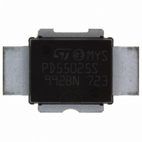
PD55025S-E STMicroelectronics, PD55025S-E Datasheet - Page 10

PD55025S-E
Manufacturer Part Number
PD55025S-E
Description
TRANS RF N-CH FET LDMOST PWRSO10
Manufacturer
STMicroelectronics
Specifications of PD55025S-E
Transistor Type
LDMOS
Frequency
500MHz
Gain
14.5dB
Voltage - Rated
40V
Current Rating
7A
Current - Test
200mA
Voltage - Test
12.5V
Power - Output
25W
Package / Case
PowerSO-10 Exposed Bottom Pad
Drain Source Voltage Vds
40V
Continuous Drain Current Id
7A
Power Dissipation Pd
79W
Operating Temperature Range
-65°C To +165°C
Channel Type
N
Channel Mode
Enhancement
Continuous Drain Current
7A
Drain Source Voltage (max)
40V
Output Power (max)
25W(Min)
Power Gain (typ)@vds
14dB
Frequency (max)
1GHz
Package Type
PowerSO-10RF (Straight lead)
Pin Count
4
Forward Transconductance (typ)
2.5S
Input Capacitance (typ)@vds
86@12.5VpF
Output Capacitance (typ)@vds
60@12.5VpF
Reverse Capacitance (typ)
6.5@12.5VpF
Operating Temp Range
-65C to 165C
Drain Efficiency (typ)
55%
Mounting
Surface Mount
Number Of Elements
1
Power Dissipation (max)
79000mW
Vswr (max)
20(Min)
Screening Level
Military
Lead Free Status / RoHS Status
Lead free / RoHS Compliant
Noise Figure
-
Lead Free Status / Rohs Status
Compliant
Other names
497-5302-5
Available stocks
Company
Part Number
Manufacturer
Quantity
Price
Company:
Part Number:
PD55025S-E
Manufacturer:
STMicroelectronics
Quantity:
2
Part Number:
PD55025S-E
Manufacturer:
ST
Quantity:
20 000
Typical performance
10/25
Figure 21. Output power vs. drain voltage
Figure 23. Output power vs. gate bias voltage Figure 24. Power gain vs. output power
Figure 25. Drain efficiency vs. output power
25
20
15
10
20
15
10
Nd (%)
70
60
50
40
30
20
10
5
0
5
0
0
7
0
8
0.5
9
VDS, DRAIN-SOURCE VOLTAGE (V)
5
VGS, GATE BIAS VOLTAGE (V)
10
1
11
1.5
500 MHz
480 MHz
Pout (W)
480 MHz
10
12
2
13
876 MHz
520 MHz
900 MHz
14
2.5
15
500 MHz
15
Idq = 150mA
Vdd = 12.5V
915 MHz
V
Pin = .5 W
DD
Idq = 150mA
Pin = .5 W
= 12.5 V
3
Doc ID 12596 Rev 2
16
520 MHz
20
17
3.5
Figure 22. Drain efficiency vs. drain voltage
Figure 26. Input return Loss vs. output power
Rl (dB)
-10
-20
-30
Gp (dB)
16
15
14
13
12
10
0
11
70
60
50
40
30
0
0
900 MHz
7
876 MHz
915 MHz
8
500 MHz
9
5
5
VDS, DRAIN-SOURCE VOLTAGE (V)
10
11
520 MHz
Pout (W)
Pout (W)
PD55015-E, PD55015S-E
10
10
12
13
480 MHz
14
15
15
915 MHz
15
Idq = 150mA
Vdd = 12.5V
Idq = 150mA
Vdd = 12.5V
876 MHz
Idq = 150mA
Pin = .5 W
900 MHz
16
20
17
20


