MRF6VP3450HR5 Freescale Semiconductor, MRF6VP3450HR5 Datasheet - Page 17
MRF6VP3450HR5
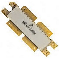
Manufacturer Part Number
MRF6VP3450HR5
Description
MOSFET RF N-CH 50V NI-1230
Manufacturer
Freescale Semiconductor
Datasheet
1.MRF6VP3450HR5.pdf
(18 pages)
Specifications of MRF6VP3450HR5
Transistor Type
2 N-Channel (Dual)
Frequency
860MHz
Gain
22.5dB
Voltage - Rated
110V
Current Rating
10µA
Current - Test
1.4A
Voltage - Test
50V
Power - Output
90W
Package / Case
NI-1230
Drain Source Voltage Vds
110V
Rf Transistor Case
NI-1230
Termination Type
SMD
Output Power Pout
90W
Peak Reflow Compatible (260 C)
Yes
Transistor Polarity
N Channel
Rohs Compliant
Yes
Filter Terminals
SMD
Gate-source Voltage
10V
Leaded Process Compatible
Yes
Operating Frequency Max
860MHz
Lead Free Status / RoHS Status
Lead free / RoHS Compliant
Noise Figure
-
Other names
MRF6VP3450HR5TR
Available stocks
Company
Part Number
Manufacturer
Quantity
Price
Company:

Part Number:
MRF6VP3450HR5
Manufacturer:
Freescale Semiconductor
Quantity:
135
Part Number:
MRF6VP3450HR5
Manufacturer:
FREESCALE
Quantity:
20 000


RF Device Data
Freescale Semiconductor
Application Notes
• AN1955: Thermal Measurement Methodology of RF Power Amplifiers
Engineering Bulletins
• EB212: Using Data Sheet Impedances for RF LDMOS Devices
Software
• Electromigration MTTF Calculator
• RF High Power Model
For Software, do a Part Number search at http://www.freescale.com, and select the “Part Number” link. Go to the Software &
Tools tab on the part’s Product Summary page to download the respective tool.
Revision
Refer to the following documents to aid your design process.
The following table summarizes revisions to this document.
2.1
0
1
2
3
4
Sept. 2008
Aug. 2008
Nov. 2008
July 2008
July 2009
Apr. 2010
Date
• Initial Release of Data Sheet
• Corrected component designation part number for C34, 35 in Table 5. Test Circuit Component Designation
• Added Note to Fig. 4, Capacitance versus Drain--Source Voltage and Fig. 5, DC Safe Operating Area to
• Adjusted imaginary component signs in Fig. 24, Series Equivalent Source and Load Impedance data table
• Fig. 24, Series Equivalent Source and Load Impedance, corrected Z
• Corrected Fig. 24 Revision History Z
•
• Added thermal resistance at 450 W CW, Thermal Characteristics table, p. 2
• Corrected Fig. 23, MTTF versus Junction Temperature, to match values given by the MRF6VP3450H/HS
• Added Electromigration MTTF Calculator and RF High Power Model availability to Product Software, p. 17
• Operating Junction Temperature increased from 200°C to 225°C in Maximum Ratings table and related
• Reporting of pulsed thermal data now shown using the Z
• Fig. 2, Test Circuit Schematic, Z--list, corrected Z4, Z5 from 1.400″ x 0.590″ Microstrip to 1.400″ x 0.059″
and Values, p. 5
denote that each side of device is measured separately, p. 7
and replotted data, p. 12
impedance as measured from gate to gate, balanced configuration” and Z
impedance as measured from gate to gate, balanced configuration”, p. 12
drain, balanced configuration”, p. 12
Added capability of handli
MTTF calculator, p. 11
“Continuous use at maximum temperature will affect MTTF” footnote added, p. 1
Microstrip, p. 4
PRODUCT DOCUMENTATION AND SOFTWARE
MRF6VP3450HR6 MRF6VP3450HR5 MRF6VP3450HSR6 MRF6VP3450HSR5
REVISION HISTORY
ng 10:1 VSWR @ 50 Vdc, 850 MHz, 450 Watts CW, p. 1
load
copy to read ”Test circuit impedance as measured from drain to
Description
θJC
symbol, p. 2
source
load
copy to read ”Test circuit
copy to read ”Test circuit
17
Related parts for MRF6VP3450HR5
Image
Part Number
Description
Manufacturer
Datasheet
Request
R

Part Number:
Description:
Manufacturer:
Freescale Semiconductor, Inc
Datasheet:
Part Number:
Description:
Manufacturer:
Freescale Semiconductor, Inc
Datasheet:
Part Number:
Description:
Manufacturer:
Freescale Semiconductor, Inc
Datasheet:
Part Number:
Description:
Manufacturer:
Freescale Semiconductor, Inc
Datasheet:
Part Number:
Description:
Manufacturer:
Freescale Semiconductor, Inc
Datasheet:
Part Number:
Description:
Manufacturer:
Freescale Semiconductor, Inc
Datasheet:
Part Number:
Description:
Manufacturer:
Freescale Semiconductor, Inc
Datasheet:
Part Number:
Description:
Manufacturer:
Freescale Semiconductor, Inc
Datasheet:
Part Number:
Description:
Manufacturer:
Freescale Semiconductor, Inc
Datasheet:
Part Number:
Description:
Manufacturer:
Freescale Semiconductor, Inc
Datasheet:
Part Number:
Description:
Manufacturer:
Freescale Semiconductor, Inc
Datasheet:
Part Number:
Description:
Manufacturer:
Freescale Semiconductor, Inc
Datasheet:
Part Number:
Description:
Manufacturer:
Freescale Semiconductor, Inc
Datasheet:
Part Number:
Description:
Manufacturer:
Freescale Semiconductor, Inc
Datasheet:
Part Number:
Description:
Manufacturer:
Freescale Semiconductor, Inc
Datasheet: