ATF-33143-TR1G Avago Technologies US Inc., ATF-33143-TR1G Datasheet
ATF-33143-TR1G
Specifications of ATF-33143-TR1G
Available stocks


Related parts for ATF-33143-TR1G


ATF-33143-TR1G Summary of contents
Page 1
... MHz to 10 GHz frequency range. Note: 1. From the same PHEMT FET family, the smaller geometry ATF- 34143 may also be considered for the higher gain performance, particularly in the higher frequency band (1.8 GHz and up). ...
Page 2
... ATF-33143 Absolute Maximum Ratings Symbol Parameter V Drain - Source Voltage DS V Gate - Source Voltage GS V Gate Drain Voltage [ Drain Current [ Total Power Dissipation diss P RF Input Power in max T Channel Temperature CH T Storage Temperature STG θ Thermal Resistance [6] jc Product Consistency Distribution Charts 500 +0 ...
Page 3
... ATF-33143 DC Electrical Specifications Symbol Parameters and Test Conditions [1] I Saturated Drain Current dss V [1] Pinchoff Voltage P I Quiescent Bias Current d g [1] Transconductance m I Gate to Drain Leakage Current GDO I Gate Leakage Current gss NF Noise Figure G Associated Gain [3] a Output 3 rd Order OIP3 ...
Page 4
... ATF-33143 Typical Performance Curves 100 120 I (mA) DSQ Figure 6. OIP3, IIP3 vs. Bias at 2 GHz. [ 100 120 I (mA) DSQ Figure 8. P vs. Bias at 2 GHz. [1,2] 1dB 100 120 I (mA) DSQ Figure 10. NF and G vs. Bias at 2 GHz. [1] a Notes: 1. Measurements made on a fixed tuned production test board that was tuned for optimal gain match with reasonable noise figure bias ...
Page 5
... ATF-33143 Typical Performance Curves, 1 1.0 0 FREQUENCY (GHz) Figure 12. F vs. Frequency and Current at 4V. min 25 2.0 25C -40C 85C 20 1.5 15 1 FREQUENCY (GHz) Figure 14. F and G vs. Frequency and Temp at min 3.0 1dB OIP3 Gain 25 2.5 NF 2.0 20 1.5 15 1.0 10 0.5 ...
Page 6
... ATF-33143 Typical Performance Curves 100 120 I (mA) DS [1] Figure 18. P vs. I Active Bias Tuned for NF @ 1dB DS 4V GHz. Note: 1. Measurements made on a fixed tuned test board that was tuned for optimal gain match with reasonable noise figure bias. This circuit represents a trade-off between an optimal noise match, maximum gain match and a realizable match based on production test board requirements ...
Page 7
... ATF-33143 Power Parameters Tuned for Max P Freq P I 1dB d (GHz) (dBm) (mA) 0.9 20.7 89 1.5 21.2 91 1.8 21.1 80 2.0 21.6 81 4.0 23.0 97 6.0 24.0 130 70 P out 60 Gain PAE -10 -20 -40 -30 -20 - (dBm) in Figure 20. Swept Power Tuned for Max P 1dB V =4V mA, 2 GHz. ...
Page 8
... Notes: 1. The F values are based on a set of 16 noise figure measurements made at 16 different impedances using an ATF NP5 test system. From these min measurements a true F is calculated. Refer to the noise parameter application section for more information. min 2. S and noise parameters are measured on a microstrip line made on 0.025 inch thick alumina carrier. The input reference plane is at the end of the gate lead ...
Page 9
... Notes: 1. The F values are based on a set of 16 noise figure measurements made at 16 different impedances using an ATF NP5 test system. From these min measurements a true F is calculated. Refer to the noise parameter application section for more information. min 2. S and noise parameters are measured on a microstrip line made on 0.025 inch thick alumina carrier. The input reference plane is at the end of the gate lead ...
Page 10
... Notes: 1. The F values are based on a set of 16 noise figure measurements made at 16 different impedances using an ATF NP5 test system. From these min measurements a true F is calculated. Refer to the noise parameter application section for more information. min 2. S and noise parameters are measured on a microstrip line made on 0.025 inch thick alumina carrier. The input reference plane is at the end of the gate lead ...
Page 11
... Notes: 1. The F values are based on a set of 16 noise figure measurements made at 16 different impedances using an ATF NP5 test system. From these min measurements a true F is calculated. Refer to the noise parameter application section for more information. min 2. S and noise parameters are measured on a microstrip line made on 0.025 inch thick alumina carrier. The input reference plane is at the end of the gate lead ...
Page 12
... Notes: 1. The F values are based on a set of 16 noise figure measurements made at 16 different impedances using an ATF NP5 test system. From these min measurements a true F is calculated. Refer to the noise parameter application section for more information. min 2. S and noise parameters are measured on a microstrip line made on 0.025 inch thick alumina carrier. The input reference plane is at the end of the gate lead ...
Page 13
... Notes: 1. The F values are based on a set of 16 noise figure measurements made at 16 different impedances using an ATF NP5 test system. From these min measurements a true F is calculated. Refer to the noise parameter application section for more information. min 2. S and noise parameters are measured on a microstrip line made on 0.025 inch thick alumina carrier. The input reference plane is at the end of the gate lead ...
Page 14
Noise Parameter Applications Information F values at 2 GHz and higher are based on min measurements while the F below 2 GHz have been mins extrapolated. The F values are based on a set of min 16 noise figure measurements ...
Page 15
... ATF-33143 Die Model Statz Model MESFETM1 NFET=yes Cgs=1.6 pF PFET=no Gdcap=3 Vto=–0.95 Cgd=0.32 pF Beta=0.48 Rgd= Lambda=0.09 Tqm= Alpha=4 Vmax= B=0.8 Fc= Tnom=27 Rd=.125 Idstc= Rg=1 Vbi=0.7 Rs=0.0625 Tau= Ld=0.00375 nH Betatce= Lg-0.00375 nH Delta1=0.2 Ls=0.00125 nH Delta2= Cds=0.08 pF Gscap=3 Crf=0.1 This model can be used as a design tool. It has been tested on MDS for various specifications ...
Page 16
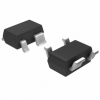
... Part Number Ordering Information No. of Part Number Devices ATF-33143-TR1G 3000 ATF-33143-TR2G 10000 ATF-33143-BLKG 100 Package Dimensions SC-70 4L/SOT-343 1.30 (.051) BSC HE 1.15 (.045) BSC DIMENSIONS (mm) SYMBOL MIN. MAX. E 1.15 1.35 D 1.85 2.25 HE 1.80 2.40 A 0.80 1.10 A2 0.80 1.00 A1 0.00 0.10 b 0.25 ...
Page 17
Recommended PCB Pad Layout for Avago’s SC70 4L/SOT-343 Products 1.30 0.051 1.00 0.039 2.00 0.60 0.079 0.024 0.9 0.035 1.15 0.045 mm Dimensions in inches Device Orientation REEL CARRIER TAPE USER FEED DIRECTION COVER TAPE 17 TOP VIEW 4 mm ...
Page 18
Tape Dimensions and Product Orientation For Outline DESCRIPTION CAVITY LENGTH WIDTH DEPTH PITCH BOTTOM HOLE DIAMETER PERFORATION DIAMETER PITCH POSITION CARRIER TAPE WIDTH THICKNESS COVER TAPE WIDTH TAPE THICKNESS DISTANCE CAVITY TO PERFORATION (WIDTH DIRECTION) CAVITY ...