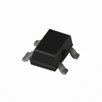
ATF-54143-TR2G Avago Technologies US Inc., ATF-54143-TR2G Datasheet - Page 14

ATF-54143-TR2G
Manufacturer Part Number
ATF-54143-TR2G
Description
IC PHEMT 2GHZ 3V 60MA SOT-343
Manufacturer
Avago Technologies US Inc.
Datasheet
1.ATF-54143-TR2G.pdf
(17 pages)
Specifications of ATF-54143-TR2G
Transistor Type
pHEMT FET
Frequency
2GHz
Gain
16.6dB
Voltage - Rated
5V
Current Rating
120mA
Noise Figure
0.5dB
Current - Test
60mA
Voltage - Test
3V
Power - Output
20.4dBm
Package / Case
SC-70-4, SC-82-4, SOT-323-4, SOT-343
Drain Source Voltage Vds
5V
Continuous Drain Current Id
120mA
Power Dissipation Pd
725mW
Noise Figure Typ
0.5dB
Rf Transistor Case
SOT-343
No. Of Pins
4
Peak Reflow Compatible (260 C)
Yes
Frequency Max
6GHz
Rohs Compliant
Yes
Drain Current Idss Max
5µA
Lead Free Status / RoHS Status
Lead free / RoHS Compliant
Available stocks
Company
Part Number
Manufacturer
Quantity
Price
Part Number:
ATF-54143-TR2G
Manufacturer:
AVAGO/安华高
Quantity:
20 000
Noise Parameter Applications
Information
F
are based on measurements
while the F
been extrapolated. The F
values are based on a set of
16 noise figure measurements
made at 16 different impedances
using an ATN NP5 test system.
From these measurements, a true
F
sents the true minimum noise
figure of the device when the
device is presented with an
impedance matching network
that transforms the source
impedance, typically 50Ω, to an
impedance represented by the
reflection coefficient G
designer must design a matching
network that will present G
the device with minimal associ-
ated circuit losses. The noise
figure of the completed amplifier
is equal to the noise figure of the
device plus the losses of the
matching network preceding the
device. The noise figure of the
device is equal to F
the device is presented with G
14
min
min
values at 2 GHz and higher
is calculated. F
mins
below 2 GHz have
min
min
o
only when
repre-
. The
min
o
to
o
.
If the reflection coefficient of the
matching network is other than
G
device will be greater than F
based on the following equation.
NF = F
Where R
noise resistance, Γ
mum reflection coefficient
required to produce F
the reflection coefficient of the
source impedance actually
presented to the device. The
losses of the matching networks
are non-zero and they will also
add to the noise figure of the
device creating a higher amplifier
noise figure. The losses of the
matching networks are related to
the Q of the components and
associated printed circuit board
loss. Γ
higher frequencies and increases
as frequency is lowered. Larger
gate width devices will typically
have a lower Γ
narrower gate width devices.
Typically for FETs, the higher Γ
usually infers that an impedance
o
, then the noise figure of the
o
min
is typically fairly low at
n
/Z
+ 4 R
o
Zo (|1 + Γ
is the normalized
n
o
as compared to
o
is the opti-
|Γ
min
o
s
|
– Γ
2
) (1 - |Γ
and Γ
o
|
2
min
s
s
o
|
is
2
)
much higher than 50Ω is required
for the device to produce F
VHF frequencies and even lower
L Band frequencies, the required
impedance can be in the vicinity
of several thousand ohms. Match-
ing to such a high impedance
requires very hi-Q components in
order to minimize circuit losses.
As an example at 900 MHz, when
airwwound coils (Q > 100) are
used for matching networks, the
loss can still be up to 0.25 dB
which will add directly to the
noise figure of the device. Using
muiltilayer molded inductors with
Qs in the 30 to 50 range results in
additional loss over the airwound
coil. Losses as high as 0.5 dB or
greater add to the typical 0.15 dB
F
amplifier noise figure of nearly
0.65 dB. A discussion concerning
calculated and measured circuit
losses and their effect on ampli-
fier noise figure is covered in
Agilent Application 1085.
min
of the device creating an
min
. At


