VRF2933 Microsemi Power Products Group, VRF2933 Datasheet

MOSFET RF PWR N-CH 50V 300W M177

VRF2933

Manufacturer Part Number
VRF2933
Description
MOSFET RF PWR N-CH 50V 300W M177
Manufacturer
Microsemi Power Products Group
Datasheet

Specifications of VRF2933

Transistor Type
N-Channel
Frequency
30MHz
Gain
22dB
Voltage - Rated
170V
Current Rating
40A
Current - Test
250mA
Voltage - Test
50V
Power - Output
300W
Package / Case
M177
Lead Free Status / RoHS Status
Lead free / RoHS Compliant
Noise Figure
-
Other names
VRF2933MP
VRF2933MP

Available stocks

Company
Part Number
Manufacturer
Quantity
Price
Part Number:
VRF2933
Manufacturer:
ST
Quantity:
43
Part Number:
VRF2933
Manufacturer:
ST
0
Part Number:
VRF2933
Manufacturer:
MICROSEMI/美高森美
Quantity:
20 000
Part Number:
VRF2933MP
Manufacturer:
MICROSEMI/美高森美
Quantity:
20 000
Maximum Ratings
The VRF2933 is a gold-metallized silicon n-channel RF power transistor de-
signed for broadband commercial and military applications requiring high power
and gain without compromising reliability, ruggedness, or inter-modulation
distortion.
Static Electrical Characteristics
Thermal Characteristics
FEATURES
• Improved Ruggedness V
• 300W with 20dB Min. Gain @ 30MHz, 50V
• Excellent Stability & Low IMD
• Common Source Confi guration
• RoHS Compliant
Symbol
Symbol
Symbol
V
RF POWER VERTICAL MOSFET
V
V
CAUTION: These Devices are Sensitive to Electrostatic Discharge. Proper Handling Procedures Should Be Followed.
R
(BR)DSS
I
V
T
DS(ON)
I
GS(TH)
V
DSS
GSS
g
P
T
I
θ JC
STG
DSS
fs
D
GS
D
J
Parameter
Drain-Source Breakdown Voltage (V
On State Drain Voltage (I
Zero Gate Voltage Drain Current (V
Gate-Source Leakage Current (V
Forward Transconductance (V
Gate Threshold Voltage (V
Characteristic
Junction to Case Thermal Resistance
Parameter
Drain-Source Voltage
Continuous Drain Current @ T
Gate-Source Voltage
Total Device dissipation @ T
Storage Temperature Range
Operating Junction Temperature Max
(BR)DSS
= 170V
D(ON)
DS
Microsemi Website - http://www.microsemi.com
= 10V, I
C
= 20A, V
DS
= 25°C
C
= 10V, I
= 25°C
DS
DS
= ±20V, V
GS
D
= 100V, V
GS
= 100mA)
= 0V, I
D
= 10V)
• 3:1 Load VSWR Capability at Specifi ed Operating Conditions
• Nitride Passivated
• Refractory Gold Metallization
• Improved Replacement for SD2933
• Thermally Enhanced Package
= 20A)
D
DS
= 100mA)
GS
= 0V)
= 0V)
All Ratings: T
C
=25°C unless otherwise specifi ed
Min
170
Min
2.9
8
-65 to 150
VRF2933
Typ
170
±40
648
200
180
2.0
3.6
Typ
40
50V, 300W, 150MHz
VRF2933
Max
Max
0.27
5.0
2.0
2.0
4.4
mhos
°C/W
Unit
Unit
Unit
mA
°C
W
μA
V
V
A
V
V

Related parts for VRF2933

VRF2933 Summary of contents

Page 1

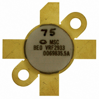
... RF POWER VERTICAL MOSFET The VRF2933 is a gold-metallized silicon n-channel RF power transistor de- signed for broadband commercial and military applications requiring high power and gain without compromising reliability, ruggedness, or inter-modulation distortion. FEATURES • Improved Ruggedness V = 170V (BR)DSS • 300W with 20dB Min. Gain @ 30MHz, 50V • ...

Page 2

... Typ Max Degradation in Output Power 250μs PULSE TEST<0.5 % DUTY CYCLE T = -55° 25° 125° DRAIN-TO-SOURCE VOLTAGE (V) DS FIGURE 2, Transfer Characteristics I DMax R ds(on) PD Max = T 125° 75° 100 800 V , DRAIN-TO-SOURCE VOLTAGE (V) DS FIGURE 4, Forward Safe Operating Area VRF2933 Unit pF Unit ...

Page 3

... Freq=65MHz 450 400 350 300 250 200 150 100 INPUT POWER (WATTS PEP) out Figure 23 5.5 4 0.1 7 10.1 3 0.6 3 6.0 3 1.1 3 1.5 2 4.0 1. 2.07 2 1.9 1 0.66 1. 0.2 1. 0 250mA dq =150V dd VRF2933 1.0 50V 40V versus P OUT IN out ...

Page 4

... C11 C10 T2 Output C8 C7 DIM MIN TYP MAX A 0.225 0.230 0.235 B 0.265 0.270 0.275 C 0.860 0.865 0.870 D 1.130 1.135 1.140 0.545 0.550 0.555 E F 0.003 0.005 0.007 G 0.098 0.103 0.108 H 0.150 0.160 0.170 I 0.280 J 1.080 1.100 1.120 K 0.625 0.630 0.635 VRF2933 ...

Related keywords