BLA1011-200,112 NXP Semiconductors, BLA1011-200,112 Datasheet - Page 3
BLA1011-200,112
Manufacturer Part Number
BLA1011-200,112
Description
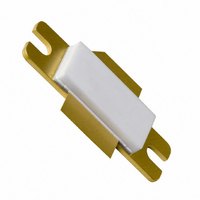
TRANS LDMOS NCH 75V SOT502A
Manufacturer
NXP Semiconductors
Datasheet
1.BLA1011-200112.pdf
(13 pages)
Specifications of BLA1011-200,112
Transistor Type
LDMOS
Frequency
1.03GHz
Gain
13dB
Voltage - Rated
75V
Current Rating
1µA
Current - Test
150mA
Voltage - Test
36V
Power - Output
200W
Package / Case
SOT502A
Configuration
Single
Transistor Polarity
N-Channel
Resistance Drain-source Rds (on)
0.06 Ohms
Drain-source Breakdown Voltage
75 V
Gate-source Breakdown Voltage
+/- 22 V
Power Dissipation
700 W
Maximum Operating Temperature
+ 200 C
Mounting Style
SMD/SMT
Minimum Operating Temperature
- 65 C
Application
Avionics
Channel Type
N
Channel Mode
Enhancement
Drain Source Voltage (max)
75V
Output Power (max)
250W(Typ)
Power Gain (typ)@vds
15@36VdB
Frequency (min)
1.03GHz
Frequency (max)
1.09GHz
Package Type
LDMOST
Pin Count
3
Forward Transconductance (typ)
9S
Drain Source Resistance (max)
60(Typ)@9Vmohm
Operating Temp Range
-65C to 200C
Drain Efficiency (typ)
50%
Mounting
Screw
Mode Of Operation
Class-AB
Number Of Elements
1
Power Dissipation (max)
700000mW
Vswr (max)
5
Screening Level
Military
Lead Free Status / RoHS Status
Lead free / RoHS Compliant
Noise Figure
-
Lead Free Status / Rohs Status
Details
Other names
934056468112
BLA1011-200
BLA1011-200
BLA1011-200
BLA1011-200


Philips Semiconductors
5. Thermal characteristics
6. Characteristics
7. Application information
9397 750 14634
Product data sheet
7.1 Ruggedness in class-AB operation
Table 5:
[1]
Table 6:
T
Table 7:
RF performance in a common source pulsed class-AB circuit; (t
and 1090 MHz; T
The BLA1011-200 and BLA1011S-200 are capable of withstanding a load mismatch
corresponding to VSWR = 5 : 1 through all phases under the following conditions:
V
Symbol
Z
Symbol Parameter
V
V
I
I
I
g
R
Symbol
V
P
G
t
t
DSS
DSX
GSS
r
f
j
fs
DS
th(j-h)
D
(BR)DSS
GS(th)
DS
L
DS(on)
p
= 25 C unless otherwise specified
Thermal resistance is determined under RF operating conditions; t
= 36 V; f = 1030 MHz to 1090 MHz at rated load power.
drain-source breakdown voltage V
gate-source threshold voltage
drain leakage current
drain cut-off current
gate leakage current
transfer conductance
drain-source on-state resistance V
Parameter
thermal impedance from junction to heatsink T
Parameter
drain-source voltage
load power
power gain
drain efficiency
rise time
fall time
Thermal characteristics
Characteristics
Application information
h
= 25 C; Z
Rev. 08 — 26 October 2005
th(mb-h)
BLA1011-200; BLA1011S-200
= 0.15 K/W; I
Conditions
t
P
t
p
p
L
= 50 s; = 2 %
= 50 s; = 2 %
= 200 W
Conditions
V
V
V
V
V
V
GS
DS
GS
GS
DS
GS
DS
GS
= 10 V; I
= 10 V
= 10 V; I
= 0 V; I
= 0 V; V
= V
= 20 V; V
= 9 V; I
Dq
= 150 mA; unless otherwise specified.
GS(th)
D
D
DS
D
D
= 3 mA
= 10 A
+ 9 V;
Conditions
= 300 mA
= 10 A
h
DS
= 36 V
= 25 C
= 0 V
p
p
© Koninklijke Philips Electronics N.V. 2005. All rights reserved.
= 50 s,
= 50 s; = 2 %); f = 1030 MHz
Min
-
-
13
45
-
-
Avionics LDMOS transistor
= 10 %.
Min
75
4
-
45
-
-
-
Typ
36
200
-
-
-
-
[1]
Typ
0.15
Typ
-
-
-
-
-
9
60
Max
-
50
50
Max Unit
-
5
1
-
1
-
-
Unit
K/W
Unit
V
W
dB
%
ns
ns
3 of 13
V
V
A
S
m
A
A
Related parts for BLA1011-200,112
Image
Part Number
Description
Manufacturer
Datasheet
Request
R

Part Number:
Description:
MOSFET Power BULK TNS-MICP
Manufacturer:
NXP Semiconductors
Datasheet:

Part Number:
Description:
TRANS LDMOS NCH 75V SOT538A
Manufacturer:
NXP Semiconductors
Datasheet:

Part Number:
Description:
200 W LDMOS avionics power transistor for transmitter applications at frequencies from 1030 MHz to 1090 MHz
Manufacturer:
NXP Semiconductors
Datasheet:

Part Number:
Description:
MOSFET Power BULK TNS-MICP
Manufacturer:
NXP Semiconductors
Datasheet:
Part Number:
Description:
MOSFET Power BULK TNS-MICP
Manufacturer:
NXP Semiconductors
Datasheet:

Part Number:
Description:
MOSFET Power LDMOS TNS
Manufacturer:
NXP Semiconductors
Datasheet:

Part Number:
Description:
TRANS LDMOS NCH 75V SOT467C
Manufacturer:
NXP Semiconductors
Datasheet:

Part Number:
Description:
TRANS LDMOS NCH 75V SOT957A
Manufacturer:
NXP Semiconductors
Datasheet:

Part Number:
Description:
TRANS LDMOS NCH 75V SOT502A
Manufacturer:
NXP Semiconductors
Datasheet:
Part Number:
Description:
NXP Semiconductors designed the LPC2420/2460 microcontroller around a 16-bit/32-bitARM7TDMI-S CPU core with real-time debug interfaces that include both JTAG andembedded trace
Manufacturer:
NXP Semiconductors
Datasheet:

Part Number:
Description:
NXP Semiconductors designed the LPC2458 microcontroller around a 16-bit/32-bitARM7TDMI-S CPU core with real-time debug interfaces that include both JTAG andembedded trace
Manufacturer:
NXP Semiconductors
Datasheet:
Part Number:
Description:
NXP Semiconductors designed the LPC2468 microcontroller around a 16-bit/32-bitARM7TDMI-S CPU core with real-time debug interfaces that include both JTAG andembedded trace
Manufacturer:
NXP Semiconductors
Datasheet:
Part Number:
Description:
NXP Semiconductors designed the LPC2470 microcontroller, powered by theARM7TDMI-S core, to be a highly integrated microcontroller for a wide range ofapplications that require advanced communications and high quality graphic displays
Manufacturer:
NXP Semiconductors
Datasheet:
Part Number:
Description:
NXP Semiconductors designed the LPC2478 microcontroller, powered by theARM7TDMI-S core, to be a highly integrated microcontroller for a wide range ofapplications that require advanced communications and high quality graphic displays
Manufacturer:
NXP Semiconductors
Datasheet:
Part Number:
Description:
The Philips Semiconductors XA (eXtended Architecture) family of 16-bit single-chip microcontrollers is powerful enough to easily handle the requirements of high performance embedded applications, yet inexpensive enough to compete in the market for hi
Manufacturer:
NXP Semiconductors
Datasheet: