PD85025STR-E STMicroelectronics, PD85025STR-E Datasheet
PD85025STR-E
Specifications of PD85025STR-E
Available stocks


Related parts for PD85025STR-E


PD85025STR-E Summary of contents
Page 1
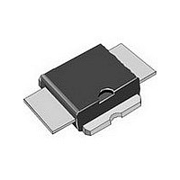
... RF performances and ease of assembly. Mounting recommendations are available in www.st.com/rf/ (look for application note AN1294) Table 1. Device summary Order codes PD85025-E PD85025S-E PD85025TR-E PD85025STR-E August 2008 RF power transistor, LdmoST plastic family Figure 1. Pin connection Gate Package PowerSO-10RF (formed lead) PowerSO-10RF (straight lead) ...
Page 2
Contents Contents 1 Electrical data . . . . . . . . . . . . . . . . . . . . . . . . . . . . . . . . . . . ...
Page 3
PD85025-E, PD85025S-E 1 Electrical data 1.1 Maximum ratings Table 2. Absolute maximum ratings (T Symbol V (BR)DSS DISS STG 1.2 Thermal data Table 3. Thermal data Symbol R thJC CASE Parameter Drain-source ...
Page 4
Electrical characteristics 2 Electrical characteristics T = +25 CASE 2.1 Static Table 4. Static Symbol DSS GSS GS( ...
Page 5
PD85025-E, PD85025S-E 3 Impedance Figure 2. Current conventions Table 8. Impedance data Frequency (MHz) 870 MHz Z (Ω) IN 0.21 +j 1.82 Impedance Z (Ω) DL 1.23 -j 0.98 5/15 ...
Page 6
Typical performance 4 Typical performance Figure 3. Capacitances vs drain voltage 120 100 Coss Crss Figure 4. DC output characteristics ...
Page 7
PD85025-E, PD85025S-E Figure 6. DC output characteristics Vgs = 4.0V Vgs = 5.0V Vgs = 6.0V Figure 8. Ouptut power and efficiency vs Input ...
Page 8
Typical performance Figure 10. Pout and drain current vs supply voltage 30 Pout Vdd (V) 8/15 Figure 11. Pout and drain current vs supply 2 ...
Page 9
PD85025-E, PD85025S-E 5 Package mechanical data In order to meet environmental requirements, ST offers these devices in ECOPACK® packages. These packages have a lead-free second level interconnect . The category of second level interconnect is marked on the package and ...
Page 10
Package mechanical data Table 9. PowerSO-10RF formed lead (gull wing) mechanical data Dim Note: Resin protrusions not included (max ...
Page 11
PD85025-E, PD85025S-E Table 10. PowerSO-10RF straight lead mechanical data Dim Note: Resin protrusions not included (max value: 0.15 mm per side) ...
Page 12
Package mechanical data Figure 14. Tube information 12/15 PD85025-E, PD85025S-E ...
Page 13
PD85025-E, PD85025S-E Figure 15. Reel information Package mechanical data 13/15 ...
Page 14
Revision history 6 Revision history Table 11. Document revision history Date 21-May-2007 26-Aug-2008 14/15 Revision 1 Initial release. 2 Updated Table 4 on page 4 PD85025-E, PD85025S-E Changes ...
Page 15
... PD85025-E, PD85025S-E Information in this document is provided solely in connection with ST products. STMicroelectronics NV and its subsidiaries (“ST”) reserve the right to make changes, corrections, modifications or improvements, to this document, and the products and services described herein at any time, without notice. All ST products are sold pursuant to ST’s terms and conditions of sale. ...