AT-41486-BLKG Avago Technologies US Inc., AT-41486-BLKG Datasheet - Page 2
AT-41486-BLKG
Manufacturer Part Number
AT-41486-BLKG
Description
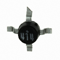
TRANS SIL LOW NOISE BIPOL 45MD
Manufacturer
Avago Technologies US Inc.
Type
Low Noiser
Specifications of AT-41486-BLKG
Package / Case
4-SMD (86 Plastic)
Transistor Type
NPN
Voltage - Collector Emitter Breakdown (max)
12V
Frequency - Transition
8GHz
Noise Figure (db Typ @ F)
1.4dB ~ 3dB @ 1GHz ~ 4GHz
Gain
9dB ~ 18dB
Power - Max
500mW
Dc Current Gain (hfe) (min) @ Ic, Vce
30 @ 10mA, 8V
Current - Collector (ic) (max)
60mA
Mounting Type
Surface Mount
Dc Collector/base Gain Hfe Min
30 at 10 mA at 8 V
Configuration
Single Dual Emitter
Transistor Polarity
NPN
Mounting Style
SMD/SMT
Collector- Emitter Voltage Vceo Max
12 V
Emitter- Base Voltage Vebo
1.5 V
Continuous Collector Current
60 mA
Maximum Dc Collector Current
0.06 A
Power Dissipation
500 mW
Maximum Operating Frequency
8000 MHz
Maximum Operating Temperature
+ 150 C
Current, Collector
60 mA
Current, Gain
150
Frequency
8 GHz
Package Type
86 Plastic
Polarity
NPN
Primary Type
Si
Resistance, Thermal, Junction To Case
165 °C/W
Voltage, Breakdown, Collector To Emitter
12 V
Voltage, Collector To Base
20 V
Voltage, Collector To Emitter
12 V
Voltage, Emitter To Base
1.5 V
Lead Free Status / RoHS Status
Lead free / RoHS Compliant
Lead Free Status / RoHS Status
Lead free / RoHS Compliant, Lead free / RoHS Compliant
Other names
516-1857
AT-41486-BLKG
AT-41486-BLKG
Available stocks
Company
Part Number
Manufacturer
Quantity
Price
Company:

Part Number:
AT-41486-BLKG
Manufacturer:
AVAGO
Quantity:
11 450
Part Number:
AT-41486-BLKG
Manufacturer:
AVAGO/安华高
Quantity:
20 000


AT-41486 Absolute Maximum Ratings
Ordering Information
Note: Order part number with a “G” suffix if lead-free option
is desired.
Electrical Specifications, T
Note:
1. For this test, the emitter is grounded.
Symbol
|S
P
G
NF
G
f
h
I
I
C
Symbol
Part Numbers
AT-41486-BLK
AT-41486-BLKG
AT-41486-TR1
AT-41486-TR1G
AT-41486-TR2
AT-41486-TR2G
T
CBO
EBO
1 dB
FE
CB
1 dB
A
21E
V
V
V
T
O
P
EBO
CBO
CEO
I
T
STG
C
|
T
j
2
Insertion Power Gain; V
Power Output @ 1 dB Gain Compression
V
1 dB Compressed Gain; V
Optimum Noise Figure: V
Gain @ NF
Gain Bandwidth Product: V
Forward Current Transfer Ratio; V
Collector Cutoff Current; V
Emitter Cutoff Current; V
Collector Base Capacitance
CE
= 8 V, I
Emitter-Base Voltage
Collector-Base Voltage
Collector-Emitter Voltage
Collector Current
Power Dissipation
Junction Temperature
Storage Temperature
Parameter
O
C
; V
No. of Devices
= 25 mA
CE
Parameters and Test Conditions
= 8 V, I
1000
1000
4000
4000
A
100
100
= 25°C
[2,3]
CE
C
CE
CE
EB
= 10 mA
= 8 V, I
CB
CE
[1]
= 8 V, I
= 8 V, I
= 1 V
: V
= 8 V
= 8 V, I
Comments
CB
C
13" Reel
13" Reel
7" Reel
7" Reel
CE
Units
C
= 8 V, f = 1 MHz
C
= 25 mA
Bulk
Bulk
mW
mA
°C
°C
= 10 mA
= 25 mA
V
V
V
C
= 8 V, I
= 25 mA
C
Maximum
= 10 mA
Absolute
-65 to 150
500
150
1.5
20
12
60
f = 1.0 GHz
f = 2.0 GHz
f = 2.0 GHz
f = 2.0 GHz
f = 1.0 GHz
f = 2.0 GHz
f = 4.0 GHz
f = 1.0 GHz
f = 2.0 GHz
f = 4.0 GHz
[1]
Notes:
1. Permanent damage may occur if
2. T
3. Derate at 6 mW/°C for
4. See MEASUREMENTS section
any of these limits are exceeded.
T
“Thermal Resistance” for more
information.
CASE
C
2
Thermal Resistance
> 68°C.
Units
dBm
GHz
dB
dB
dB
dB
µA
µA
pF
—
= 25°C.
θ
jc
= 165°C/W
Min.
17.0
30
Typ. Max.
17.5
11.5
18.0
13.5
18.0
13.0
0.25
150
1.4
1.7
3.0
9.0
8.0
[2,4]
270
1.8
0.2
1.0
:
Related parts for AT-41486-BLKG
Image
Part Number
Description
Manufacturer
Datasheet
Request
R

Part Number:
Description:
TRANS NPN BIPO 12V 60MA 86-SMD
Manufacturer:
Avago Technologies US Inc.
Datasheet:

Part Number:
Description:
TRANS SIL LOW NOISE BIPOLAR 86PL
Manufacturer:
Avago Technologies US Inc.

Part Number:
Description:
BJT (Bipolar Junction Transistor)
Manufacturer:
Avago Technologies US Inc.

Part Number:
Description:
SPEAKER 8OHM .15W 72DB 30MMPC MT
Manufacturer:
PUI Audio, Inc.
Datasheet:

Part Number:
Description:
OPTOCOUPLER GATE DRV 2A 16-SOIC
Manufacturer:
Avago Technologies US Inc.
Datasheet:
Part Number:
Description:
OPTOCOUPLER 2CH 2.5A 16-SOIC
Manufacturer:
Avago Technologies US Inc.
Datasheet:

Part Number:
Description:
OPTOCOUPLER GATE DRV 0.4A 16SOIC
Manufacturer:
Avago Technologies US Inc.
Datasheet:

Part Number:
Description:
OPTOCOUPLER 2.0A 250KHZ 8-DIP
Manufacturer:
Avago Technologies US Inc.
Datasheet:

Part Number:
Description:
OPTOCOUPLER 2.0A 250KHZ GW 8-SMD
Manufacturer:
Avago Technologies US Inc.
Datasheet:

Part Number:
Description:
OPTOCOUPLER 2CH 15MBD 3.3V 8SOIC
Manufacturer:
Avago Technologies US Inc.
Datasheet:
Part Number:
Description:
OPTOCOUPLER DARL-OUT 8-DIP
Manufacturer:
Avago Technologies US Inc.
Datasheet:
Part Number:
Description:
OPTOCOUPLER IGBT DRIVE 0.4A 8DIP
Manufacturer:
Avago Technologies US Inc.
Datasheet:
Part Number:
Description:
OPTOCOUPLER DARL-OUT 8-DIP
Manufacturer:
Avago Technologies US Inc.
Datasheet: