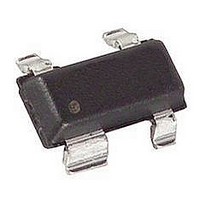
AT-32011-BLKG Avago Technologies US Inc., AT-32011-BLKG Datasheet - Page 3

AT-32011-BLKG
Manufacturer Part Number
AT-32011-BLKG
Description
TRANS NPN BIPO 5.5V 32MA SOT-143
Manufacturer
Avago Technologies US Inc.
Specifications of AT-32011-BLKG
Transistor Type
NPN
Voltage - Collector Emitter Breakdown (max)
5.5V
Noise Figure (db Typ @ F)
1dB ~ 1.3dB @ 900MHz
Gain
12.5dB ~ 14dB
Power - Max
200mW
Dc Current Gain (hfe) (min) @ Ic, Vce
70 @ 2mA, 2.7V
Current - Collector (ic) (max)
32mA
Mounting Type
Surface Mount
Package / Case
SOT-143, SOT-143B, TO-253AA
Transistor Polarity
NPN
Collector Emitter Voltage V(br)ceo
5.5V
Transition Frequency Typ Ft
10GHz
Power Dissipation Pd
200mW
Dc Collector Current
320mA
Dc Current Gain Hfe
300
Lead Free Status / RoHS Status
Lead free / RoHS Compliant
Frequency - Transition
-
Lead Free Status / RoHS Status
Lead free / RoHS Compliant, Lead free / RoHS Compliant
Available stocks
Company
Part Number
Manufacturer
Quantity
Price
Part Number:
AT-32011-BLKG
Manufacturer:
AVAGO/安华高
Quantity:
20 000
Characterization Information, T
Figure 2. AT-32011 and AT-32033 Minimum Noise Fig-
ure vs. Frequency and Current at V
Figure 5. AT-32011 and AT-32033 Power at 1 dB Gain
Compression vs. Frequency and Current at V
3
1.5
0.5
20
15
10
Symbol
-5
|S
5
0
2
1
0
G
P
0
0
IP
21
1dB
1dB
3
|
E
2
0.5
0.5
2 mA
5 mA
10 mA
20 mA
FREQUENCY (GHz)
FREQUENCY (GHz)
AT-32011 fig 5
AT-32011 fig 2
Parameters and Test Conditions
Power at 1 dB Gain Compression (opt tuning)
Gain at 1 dB Gain Compression (opt tuning)
Output Third Order Intercept Point (opt tuning)
Gain in 50 Ω System
1.0
V
V
V
V
CE
CE
CE
CE
1
= 2.7 V, I
= 2.7 V, I
= 2.7 V, I
= 2.7 V, I
1.5
1.5
CE
= 2.7 V.
C
C
C
C
= 20 mA
= 20 mA
= 20 mA
= 2 mA
2.0
1 mA
2 mA
5 mA
10 mA
20 mA
2
CE
= 2.7 V.
A
= 25°C
2.5
2.5
Figure 3. AT-32011 Associated Gain at Optimum Noise
Match vs. Frequency and Current at V
Figure 6. AT-32011 1 dB Compressed Gain vs. Frequen-
cy and Current at V
20
15
10
5
0
25
20
15
10
5
0
0
0
0.5
2 mA
5 mA
10 mA
20 mA
0.5
1 mA
2 mA
5 mA
10 mA
20 mA
FREQUENCY (GHz)
CE
FREQUENCY (GHz)
AT-32011 fig 6
= 2.7 V.
AT-32011 fig 3
1.0
1.0
f = 0.9 GHz
f = 0.9 GHz
f = 0.9 GHz
f = 0.9 GHz
1.5
1.5
CE
= 2.7 V.
2.0
2.0
2.5
2.5
Units
dBm
dBm
dB
dB
Figure 7. AT-32033 1 dB Compressed Gain vs. Frequen-
cy and Current at V
Figure 4. AT-32033 Associated Gain at Optimum Noise
Match vs. Frequency and Current at V
20
15
10
20
15
10
5
0
5
0
0
0
0.5
1 mA
2 mA
5 mA
10 mA
20 mA
AT-32011
0.5
2 mA
5 mA
10 mA
20 mA
16.5
Typ.
FREQUENCY (GHz)
CE
FREQUENCY (GHz)
13
24
13
AT-32011 fig 4
= 2.7 V.
AT-32011 fig 7
1.0
1.0
1.5
1.5
CE
AT-32033
= 2.7 V.
2.0
11.5
Typ.
2.0
13
15
24
2.5
2.5


