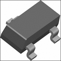
AT-41532-BLKG Avago Technologies US Inc., AT-41532-BLKG Datasheet - Page 12

AT-41532-BLKG
Manufacturer Part Number
AT-41532-BLKG
Description
TRANS NPN BIPO 12V 50MA SOT-323
Manufacturer
Avago Technologies US Inc.
Datasheet
1.AT-41532-BLKG.pdf
(14 pages)
Specifications of AT-41532-BLKG
Transistor Type
NPN
Voltage - Collector Emitter Breakdown (max)
12V
Noise Figure (db Typ @ F)
1dB ~ 1.9dB @ 900MHz ~ 2.4GHz
Gain
9dB ~ 15.5dB
Power - Max
225mW
Dc Current Gain (hfe) (min) @ Ic, Vce
30 @ 5mA, 5V
Current - Collector (ic) (max)
50mA
Mounting Type
Surface Mount
Package / Case
SC-70-3, SOT-323-3
Transistor Polarity
NPN
Collector Emitter Voltage V(br)ceo
12V
Power Dissipation Pd
225mW
Dc Collector Current
500mA
Dc Current Gain Hfe
150
Rf Transistor Case
SOT-323
No. Of Pins
3
Lead Free Status / RoHS Status
Lead free / RoHS Compliant
Frequency - Transition
-
Lead Free Status / RoHS Status
Lead free / RoHS Compliant, Lead free / RoHS Compliant
Available stocks
Company
Part Number
Manufacturer
Quantity
Price
Company:
Part Number:
AT-41532-BLKG
Manufacturer:
AVAGO
Quantity:
12 000
Part Number:
AT-41532-BLKG
Manufacturer:
AVAGO/安华高
Quantity:
20 000
Performance
The measured gain of the completed amplifier is shown in
Figure 19. The gain varies
from 14 to 15 dB over the 800 to 900 MHz frequency
range. Noise figure versus frequency is shown in Figure
20. Best performance occurs at 850 MHz providing a near
1 dB noise figure.
Measured input and output return loss is shown in Figure
21. The input return loss is 10 dB at 850 MHz and can be
improved with slight tuning at C2. Output return loss was
measured at almost 10 dB at 850 MHz.
There is considerable tuning interaction between input
and output matching networks in any single stage
amplifier. Having a somewhat better input return loss co-
incident with low noise figure may necessitate a compro-
mise in output return loss.
Output intercept point, IP
be +12 dBm. Removing the 1.1 KΩ resistor at R6 increases
IP
enhance stability; caution is urged when removing this
resistor or increasing its value without careful analysis.
Another alternative to the shunt resistor R6 would be to
incorporate a resistor in series with the transistor collector
lead. This resistor would be in the 10 to 27Ω range and
has similar effects on circuit stability. A third alternative
is to re-optimize the output match for power as opposed
to matching for lowest output VSWR. This may make the
output return loss less than 10 dB but it would enhance
power output.
Figure 19. Gain vs Frequency.
Figure 17. AT-41532 Gain vs. Frequency.
3
16
14
12
10
8
6
500
to +13.6 dBm. Resistor R6 was originally added to
600
FREQUENCY (MHz)
700
800
3
900
, was measured at 850 MHz to
1000
Figure 20. Noise Figure vs Frequency.
Figure 18. AT-41532 Noise Figure vs. Frequency.
1.6
1.5
1.4
1.3
1.2
1.1
1
500
600
FREQUENCY (MHz)
700
Modifications to Original Demo Board
The original demo board dated 01/98 requires some
modification to work as described in this application note.
The modification is to add resistor R6 in series with the
collector lead. This is accomplished by cutting the etch at
the output of Q1 such that resistor R6 can be placed on
the circuit board as shown in Figure 17. Inductor L3 will
then have be placed at a 90 degree angle with respect to
its original intended location. L3 is then connected to the
junction of R6 and L4 with a small piece of wire or etch.
Using the AT-41532 at Other Frequencies
The demo board and design techniques presented here
can be used to build low noise amplifiers for other fre-
quencies in the VHF through 1.9 GHz frequency range.
800
900
1000
Figure 21. Input/Output Return Loss.
Figure 19. Input/Output Return Loss.
-10
-12
-14
-2
-4
-6
-8
0
500
600
Input
Output
FREQUENCY (MHz)
700
800
900
1000


