MAX2602ESA+T Maxim Integrated Products, MAX2602ESA+T Datasheet
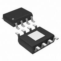
TRANS RF NPN 900MHZ 15V 8SOIC

MAX2602ESA+T

Manufacturer Part Number
MAX2602ESA+T
Description
TRANS RF NPN 900MHZ 15V 8SOIC
Manufacturer
Maxim Integrated Products
Datasheet

Specifications of MAX2602ESA+T

Transistor Type
NPN
Voltage - Collector Emitter Breakdown (max)
15V
Frequency - Transition
1GHz
Noise Figure (db Typ @ F)
3.3dB @ 836MHz
Gain
11.6dB
Power - Max
6.4W
Dc Current Gain (hfe) (min) @ Ic, Vce
100 @ 250mA, 3V
Current - Collector (ic) (max)
1.2A
Mounting Type
Surface Mount
Package / Case
8-SOIC (3.9mm Width) Exposed Pad, 8-eSOIC. 8-HSOIC
Lead Free Status / RoHS Status
Lead free / RoHS Compliant
The MAX2601/MAX2602 are RF power transistors opti-
mized for use in portable cellular and wireless equipment
that operates from three NiCd/NiMH cells or one Li-Ion
cell. These transistors deliver 1W of RF power from a
3.6V supply with efficiency of 58% when biased for con-
stant-envelope applications (e.g., FM or FSK). For NADC
(IS-54) operation, they deliver 29dBm with -28dBc ACPR
from a 4.8V supply.
The MAX2601 is a high-performance silicon bipolar RF
power transistor. The MAX2602 includes a high-
performance silicon bipolar RF power transistor, and a
biasing diode that matches the thermal and process
characteristics of the power transistor. This diode is
used to create a bias network that accurately controls
the power transistor’s collector current as the tempera-
ture changes.
The MAX2601/MAX2602 can be used as the final stage
in a discrete or module power amplifier. Silicon bipolar
technology eliminates the need for voltage inverters
and sequencing circuitry, as required by GaAsFET
power amplifiers. Furthermore, a drain switch is not
required to turn off the MAX2601/MAX2602. This
increases operating time in two ways: it allows lower
system end-of-life battery voltage, and it eliminates the
wasted power from a drain-switch device.
The MAX2601/MAX2602 are available in thermally
enhanced, 8-pin SO packages, which are screened to
the extended temperature range (-40°C to +85°C).
________________________Applications
19-1185; Rev 3; 9/08
Typical Application Circuit appears at end of data sheet.
For pricing, delivery, and ordering information, please contact Maxim Direct at 1-888-629-4642,
or visit Maxim’s website at www.maxim-ic.com.
Narrow-Band PCS (NPCS)
915MHz ISM Transmitters
Microcellular GSM (Power Class 5)
AMPS Cellular Phones
Digital Cellular Phones
Two-Way Paging
CDPD Modems
Land Mobile Radios
________________________________________________________________ Maxim Integrated Products
General Description
3.6V, 1W RF Power Transistors
for 900MHz Applications
♦ ♦ Low Voltage: Operates from 1 Li-Ion or
♦ ♦ DC-to-Microwave Operating Range
♦ ♦ 1W Output Power at 900MHz
♦ ♦ On-Chip Diode for Accurate Biasing (MAX2602)
♦ ♦ Low-Cost Silicon Bipolar Technology
♦ ♦ Does Not Require Negative Bias or Supply Switch
♦ ♦ High Efficiency: 58%
____________________________Features
MAX2601ESA
MAX2602ESA
3 NiCd/NiMH Batteries
TOP VIEW
C
B
E
E
1
2
3
4
PART
MAX2601
PSOPII
-40°C to +85°C
-40°C to +85°C
TEMP RANGE
Ordering Information
8
7
6
5
C
E
E
B
Pin Configurations
BIAS
C
B
E
1
2
3
4
MAX2602
PSOPII
PIN-PACKAGE
8 SOIC
8 SOIC
8
7
6
5
C
E
E
B
1

Related parts for MAX2602ESA+T

MAX2602ESA+T Summary of contents

Page 1

... Digital Cellular Phones Two-Way Paging CDPD Modems Land Mobile Radios Typical Application Circuit appears at end of data sheet. ________________________________________________________________ Maxim Integrated Products For pricing, delivery, and ordering information, please contact Maxim Direct at 1-888-629-4642, or visit Maxim’s website at www.maxim-ic.com. 3.6V Power Transistors for 900MHz Applications ____________________________Features ♦ ...

Page 2

RF Power Transistors for 900MHz Applications ABSOLUTE MAXIMUM RATINGS Collector-Emitter Voltage, Shorted Base (V Emitter Base Reverse Voltage (V )...................................2.3V EBO BIAS Diode Reverse Breakdown Voltage (MAX2602) ..........2.3V Average Collector Current (I )........................................1200mA C Continuous Power Dissipation (T ...

Page 3

Operating Characteristics (Test Circuit of Figure 1, input/output matching networks optimized for specific measurement frequency 30dBm 50Ω 836MHz, T OUT LOAD SOURCE COLLECTOR CURRENT 1.0 0 1.00V BB ...

Page 4

RF Power Transistors for 900MHz Applications V BB 0.1μF 1000pF 2pF L1 = COILCRAFT A05T INDUCTOR, 18.5nH T1 1", 50Ω TRANSMISSION LINE ON FR-4 Figure 1. Test Circuit _______________Detailed Description MAX2601/MAX2602 The MAX2601/MAX2602 ...

Page 5

Applications Information Optimum Port Impedance The source and load impedances presented to the MAX2601/MAX2602 have a direct impact upon its gain, output power, and linearity. Proper source- and load- terminating impedances (Z and Z S power transistor base and collector ...

Page 6

... Maxim cannot assume responsibility for use of any circuitry other than circuitry entirely embodied in a Maxim product. No circuit patent licenses are implied. Maxim reserves the right to change the circuitry and specifications without notice at any time. 6 _____________________Maxim Integrated Products, 120 San Gabriel Drive, Sunnyvale, CA 94086 408-737-7600 © 2008 Maxim Integrated Products DESCRIPTION Maxim is a registered trademark of Maxim Integrated Products, Inc ...

Related keywords