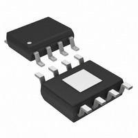
MAX2602ESA+T Maxim Integrated Products, MAX2602ESA+T Datasheet - Page 5

MAX2602ESA+T
Manufacturer Part Number
MAX2602ESA+T
Description
TRANS RF NPN 900MHZ 15V 8SOIC
Manufacturer
Maxim Integrated Products
Datasheet
1.MAX2601ESAT.pdf
(6 pages)
Specifications of MAX2602ESA+T
Transistor Type
NPN
Voltage - Collector Emitter Breakdown (max)
15V
Frequency - Transition
1GHz
Noise Figure (db Typ @ F)
3.3dB @ 836MHz
Gain
11.6dB
Power - Max
6.4W
Dc Current Gain (hfe) (min) @ Ic, Vce
100 @ 250mA, 3V
Current - Collector (ic) (max)
1.2A
Mounting Type
Surface Mount
Package / Case
8-SOIC (3.9mm Width) Exposed Pad, 8-eSOIC. 8-HSOIC
Lead Free Status / RoHS Status
Lead free / RoHS Compliant
The source and load impedances presented to the
MAX2601/MAX2602 have a direct impact upon its gain,
output power, and linearity. Proper source- and load-
terminating impedances (Z
power transistor base and collector will ensure optimum
performance.
For a power transistor, simply applying the conjugate of
the transistor’s input and output impedances calculated
from small-signal S-parameters will yield less than opti-
mum device performance.
For maximum efficiency at V
3.6V, the optimum power-transistor source and load
impedances (as defined in Figure 3) are:
Z
sented to the transistor’s base and collector. The pack-
age parasitics are dominated by inductance (as shown
in Figure 3), and need to be accounted for when calcu-
lating Z
The internal bond and package inductances shown
in Figure 3 should be included as part of the end-
application matching network, depending upon exact
layout topology.
S
At 836MHz:
At 433MHz:
and Z
S
and Z
L
reflect the impedances that should be pre-
L
Applications Information
.
Z
Z
Z
Z
S
L
S
L
_______________________________________________________________________________________
= 6.5 + j1.5
= 8.5 - j1.5
= 5.5 + j2.0
= 9.5 - j2.5
Optimum Port Impedance
S
and Z
BB
= 0.75V and V
L
) presented to the
3.6V, 1W RF Power Transistors
CC
=
for 900MHz Applications
The most important connection to make to the
MAX2601/MAX2602 is the back side. It should connect
directly to the PC board ground plane if it is on the top
side, or through numerous plated through-holes if the
ground plane is buried. For maximum gain, this con-
nection should have very little self-inductance. Since it
is also the thermal path for heat dissipation, it must
have low thermal impedance, and the ground plane
should be large.
For the latest package outline information and land patterns, go
to www.maxim-ic.com/packages.
Figure 3. Optimum Port Impedance
PACKAGE TYPE
8 SOIC
2.8nH
2.8nH
4
5
PACKAGE CODE
Z
Package Information
S
3
6
Slug Layout Techniques
MAX2601
MAX2602
S8E-12
2
7
Z
L
DOCUMENT NO.
1
8
2.8nH
2.8nH
21-0041
5


