NST45010MW6T1G ON Semiconductor, NST45010MW6T1G Datasheet

TRANSISTOR DUAL MATCHED PNP 45V

NST45010MW6T1G

Manufacturer Part Number
NST45010MW6T1G
Description
TRANSISTOR DUAL MATCHED PNP 45V
Manufacturer
ON Semiconductor
Datasheet

Specifications of NST45010MW6T1G

Transistor Type
2 PNP (Dual)
Current - Collector (ic) (max)
100mA
Voltage - Collector Emitter Breakdown (max)
45V
Vce Saturation (max) @ Ib, Ic
650mV @ 5mA, 100mA
Dc Current Gain (hfe) (min) @ Ic, Vce
220 @ 2mA, 5V
Power - Max
380mW
Frequency - Transition
100MHz
Mounting Type
Surface Mount
Package / Case
SC-70-6, SC-88, SOT-363
Configuration
Dual
Transistor Polarity
PNP
Mounting Style
SMD/SMT
Collector- Emitter Voltage Vceo Max
45 V
Emitter- Base Voltage Vebo
5 V
Maximum Dc Collector Current
0.1 A
Power Dissipation
380 mW
Maximum Operating Frequency
100 MHz
Maximum Operating Temperature
+ 150 C
Minimum Operating Temperature
- 55 C
Lead Free Status / RoHS Status
Lead free / RoHS Compliant
Current - Collector Cutoff (max)
-
Lead Free Status / Rohs Status
Lead free / RoHS Compliant

Available stocks

Company
Part Number
Manufacturer
Quantity
Price
Part Number:
NST45010MW6T1G
Manufacturer:
ON Semiconductor
Quantity:
1 850
Part Number:
NST45010MW6T1G
Manufacturer:
ON
Quantity:
30 000
Company:
Part Number:
NST45010MW6T1G
Quantity:
21 000
NST45010MW6T1G
Dual Matched General
Purpose Transistor
PNP Matched Pair
ideally suited for portable products. They are assembled to create a
pair of devices highly matched in all parameters, eliminating the need
for costly trimming. Applications are Current Mirrors; Differential,
Sense and Balanced Amplifiers; Mixers; Detectors and Limiters.
Complementary NPN equivalent NST45011MW6T1G is available.
Features
Stresses exceeding Maximum Ratings may damage the device. Maximum
Ratings are stress ratings only. Functional operation above the Recommended
Operating Conditions is not implied. Extended exposure to stresses above the
Recommended Operating Conditions may affect device reliability.
1. FR−5 = 1.0 x 0.75 x 0.062 in
© Semiconductor Components Industries, LLC, 2009
October, 2009 − Rev. 1
MAXIMUM RATINGS
THERMAL CHARACTERISTICS
Collector −Emitter Voltage
Collector −Base Voltage
Emitter −Base Voltage
Collector Current − Continuous
Total Device Dissipation
Thermal Resistance,
Junction and Storage
These transistors are housed in an ultra−small SOT−363 package
Compliant
Current Gain Matching to 10%
Base−Emitter Voltage Matched to ≤ 2 mV
Drop−In Replacement for Standard Device
These Devices are Pb−Free, Halogen Free/BFR Free and are RoHS
Per Device
FR−5 Board (Note 1)
T
Derate Above 25°C
Junction to Ambient
Temperature Range
A
= 25°C
Characteristic
Rating
Symbol
T
R
J
P
, T
qJA
D
stg
Symbol
V
V
V
CEO
CBO
EBO
I
C
−55 to +150
Max
380
250
328
3.0
Value
−100
−5.0
−45
−50
1
mW/°C
mAdc
°C/W
Unit
Unit
mW
°C
V
V
V
†For information on tape and reel specifications,
NST45010MW6T1G
including part orientation and tape sizes, please
refer to our Tape and Reel Packaging Specifications
Brochure, BRD8011/D.
(Note: Microdot may be in either location)
Device
Q
(3)
(4)
ORDERING INFORMATION
1
MARKING DIAGRAMS
4F
M
G
http://onsemi.com
= Device Code
= Date Code
= Pb−Free Package
CASE 419B
SOT−363
STYLE 1
6
(Pb−Free)
SOT−363
4F MG
Package
(5)
Publication Order Number:
G
(2)
1
NST45010MW6/D
Tape & Reel
Shipping
(1)
(6)
3000 /
Q
2

Related parts for NST45010MW6T1G

NST45010MW6T1G Summary of contents

Page 1

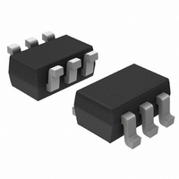
... Date Code G = Pb−Free Package (Note: Microdot may be in either location) ORDERING INFORMATION Device Package Shipping NST45010MW6T1G SOT−363 3000 / (Pb−Free) Tape & Reel including part orientation and tape sizes, please refer to our Tape and Reel Packaging Specifications Brochure, BRD8011/D. Publication Order Number: ...

Page 2

ELECTRICAL CHARACTERISTICS Characteristic OFF CHARACTERISTICS Collector −Emitter Breakdown Voltage, (I Collector −Emitter Breakdown Voltage, (I Collector −Base Breakdown Voltage Emitter −Base Breakdown Voltage −1.0 mA) E Collector Cutoff Current (V = − Collector Cutoff ...

Page 3

V = - 25°C A 1.0 0.7 0.5 0.3 0.2 -0.2 -0.5 -1.0 -2.0 -5.0 -10 - COLLECTOR CURRENT (mAdc) C Figure 1. Normalized DC Current Gain -2.0 -1.6 -1 ...

Page 4

T = 25° 25° 5.0 BONDING WIRE LIMIT THERMAL LIMIT SECOND BREAKDOWN LIMIT 2.0 1.0 5 COLLECTOR-EMITTER VOLTAGE (V) CE Figure 7. Active Region Safe Operating Area ...

Page 5

... Pb−Free strategy and soldering details, please download the ON Semiconductor Soldering and Mounting Techniques Reference Manual, SOLDERRM/D. ON Semiconductor and are registered trademarks of Semiconductor Components Industries, LLC (SCILLC). SCILLC reserves the right to make changes without further notice to any products herein ...

Related keywords