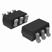
NST45010MW6T1G ON Semiconductor, NST45010MW6T1G Datasheet - Page 4

NST45010MW6T1G
Manufacturer Part Number
NST45010MW6T1G
Description
TRANSISTOR DUAL MATCHED PNP 45V
Manufacturer
ON Semiconductor
Datasheet
1.NST45010MW6T1G.pdf
(5 pages)
Specifications of NST45010MW6T1G
Transistor Type
2 PNP (Dual)
Current - Collector (ic) (max)
100mA
Voltage - Collector Emitter Breakdown (max)
45V
Vce Saturation (max) @ Ib, Ic
650mV @ 5mA, 100mA
Dc Current Gain (hfe) (min) @ Ic, Vce
220 @ 2mA, 5V
Power - Max
380mW
Frequency - Transition
100MHz
Mounting Type
Surface Mount
Package / Case
SC-70-6, SC-88, SOT-363
Configuration
Dual
Transistor Polarity
PNP
Mounting Style
SMD/SMT
Collector- Emitter Voltage Vceo Max
45 V
Emitter- Base Voltage Vebo
5 V
Maximum Dc Collector Current
0.1 A
Power Dissipation
380 mW
Maximum Operating Frequency
100 MHz
Maximum Operating Temperature
+ 150 C
Minimum Operating Temperature
- 55 C
Lead Free Status / RoHS Status
Lead free / RoHS Compliant
Current - Collector Cutoff (max)
-
Lead Free Status / Rohs Status
Lead free / RoHS Compliant
Available stocks
Company
Part Number
Manufacturer
Quantity
Price
Company:
Part Number:
NST45010MW6T1G
Manufacturer:
ON Semiconductor
Quantity:
1 850
Company:
Part Number:
NST45010MW6T1G
Manufacturer:
ON
Quantity:
30 000
200
100
5.0
2.0
50
10
1.0
Figure 7. Active Region Safe Operating Area
V
CE
BONDING WIRE LIMIT
THERMAL LIMIT
SECOND BREAKDOWN LIMIT
, COLLECTOR-EMITTER VOLTAGE (V)
5.0
T
A
= 25°C
10
T
J
1 s
= 25°C
TYPICAL CHARACTERISTICS
30
45
3 ms
http://onsemi.com
65
100
4
of the transistor that must be observed for reliable
operation. Collector load lines for specific circuits must
fall below the limits indicated by the applicable curve.
or T
The safe operating area curves indicate I
The data of Figure 7 is based upon T
A
is variable depending upon conditions.
J(pk)
C
= 150°C; T
−V
CE
limits
C


