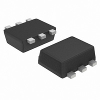
NST3906DXV6T1 ON Semiconductor, NST3906DXV6T1 Datasheet

NST3906DXV6T1
Specifications of NST3906DXV6T1
Available stocks
Related parts for NST3906DXV6T1
NST3906DXV6T1 Summary of contents
Page 1
... NST3906DXV6T1, NST3906DXV6T5 Dual General Purpose Transistor The NST3906DXV6T1 device is a spin- off of our popular SOT-23/SOT-323 three-leaded device designed for general purpose amplifier applications and is housed in the SOT- 563 six-leaded surface mount package. By putting two discrete devices in one package, this device is ideal for low-power surface mount applications where board space premium ...
Page 2
... Vdc Rise Time (I = -10 mAdc Storage Time (V = -3.0 Vdc Fall Time ( -1.0 mAdc Pulse Test: Pulse Width 300 s; Duty Cycle NST3906DXV6T1, NST3906DXV6T5 ( unless otherwise noted 1 1.0 kHz) = 0.5 Vdc -1.0 mAdc -10 mAdc) C 2.0%. http://onsemi.com 2 Symbol Min Max Unit V -40 ...
Page 3
... NST3906DXV6T1, NST3906DXV6T5 < +0 10.6 V 300 ns DUTY CYCLE = 2% Figure 1. Delay and Rise Time Equivalent Test Circuit TYPICAL TRANSIENT CHARACTERISTICS 10 7.0 5.0 3.0 2.0 1.0 0.1 500 300 200 100 1.0 2.0 3.0 5.0 7 COLLECTOR CURRENT (mA) C Figure 4. Turn - On Time 3 V +9.1 V 275 ...
Page 4
... NST3906DXV6T1, NST3906DXV6T5 TYPICAL AUDIO SMALL- SIGNAL CHARACTERISTICS (V CE 5.0 SOURCE RESISTANCE = 200 1 4.0 SOURCE RESISTANCE = 200 0 3.0 SOURCE RESISTANCE = 2 2.0 SOURCE RESISTANCE = 2.0 k 1.0 = 100 0.1 0.2 0.4 1.0 2.0 4 FREQUENCY (kHz) Figure 6. 300 200 100 0.1 0.2 0.3 0.5 0.7 1 ...
Page 5
... NST3906DXV6T1, NST3906DXV6T5 TYPICAL STATIC CHARACTERISTICS 2.0 1.0 0.7 0.5 0.3 0.2 0.1 0.1 0.2 0.3 0.5 0.7 1.0 1 0.6 0.4 0.2 0 0.01 0.02 0.03 0.05 0.07 1 BE(sat 0.8 V 0.6 0 CE(sat) C 0.2 0 1.0 2.0 5 COLLECTOR CURRENT (mA) C Figure 14. “ON” Voltages ...
Page 6
... NST3906DXV6T1, NST3906DXV6T5 INFORMATION FOR USING THE SOT-563 SURFACE MOUNT PACKAGE MINIMUM RECOMMENDED FOOTPRINT FOR SURFACE MOUNTED APPLICATIONS Surface mount board layout is a critical portion of the total design. The footprint for the semiconductor packages must be the correct size to insure proper solder connection The power dissipation of the SOT-563 is a function of the pad size ...
Page 7
... NST3906DXV6T1, NST3906DXV6T5 PACKAGE DIMENSIONS SOT-563, 6 LEAD CASE 463A-01 ISSUE - - 0.08 (0.003 STYLE 1: STYLE 2: PIN 1. EMITTER 1 PIN 1. EMITTER 1 2. BASE 1 2. EMITTER2 3. COLLECTOR 2 3. BASE 2 4. EMITTER 2 4. COLLECTOR 2 5. BASE 2 5. BASE 1 6. COLLECTOR 1 6. COLLECTOR 1 http://onsemi.com NOTES: 1. DIMENSIONING AND TOLERANCING PER ANSI Y14 ...
Page 8
... Phone: 303-675-2175 or 800-344-3860 Toll Free USA/Canada Fax: 303-675-2176 or 800-344-3867 Toll Free USA/Canada Email: ONlit@hibbertco.com N. American Technical Support: 800-282-9855 Toll Free USA/Canada NST3906DXV6T1, NST3906DXV6T5 JAPAN: ON Semiconductor, Japan Customer Focus Center 2-9-1 Kamimeguro, Meguro-ku, Tokyo, Japan 153-0051 Phone: 81-3-5773-3850 ON Semiconductor Website: http://onsemi.com For additional information, please contact your local Sales Representative ...


