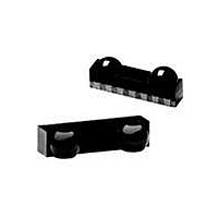
TFBS4711-TR1 Vishay, TFBS4711-TR1 Datasheet - Page 2

TFBS4711-TR1
Manufacturer Part Number
TFBS4711-TR1
Description
IRDA TX/RX 0.1152Mbps 2.5V/3.3V/5V 6-Pin SMD T/R
Manufacturer
Vishay
Type
TX/RXr
Specifications of TFBS4711-TR1
Package
6SMD
Maximum Communication Distance
100(Typ) cm
Half Intensity Angle Degrees
44 °
Maximum Data Rate
0.1152 Mbps
Peak Wavelength
900(Max) nm
Pulse Width
2 us
Radiant Intensity
60 mW/sr
Operating Supply Voltage
2.4 to 5.5 V
Wavelength
900 nm
Continual Data Transmission
115.2 Kbit/s
Transmission Distance
1 m
Maximum Rise Time
100 ns
Maximum Fall Time
100 ns
Led Supply Voltage
- 0.5 V to 6 V
Operating Voltage
2.4 V to 5.5 V
Maximum Operating Temperature
+ 85 C
Minimum Operating Temperature
- 25 C
Dimensions
6 mm x 3.1 mm x 1.9 mm
Data Rate Max
115.2Kbps
Data Transmission Distance
1m
Supply Current
600µA
Supply Voltage Range
2.4V To 5.5V
Operating Temperature Range
-25°C To +85°C
External Depth
1.9mm
Rohs Compliant
Yes
Communication Cone
15°
Data Rate
115.2kbs (SIR)
Idle Current, Typ @ 25° C
75µA
Link Range, Low Power
1m
Operating Temperature
-30°C ~ 85°C
Orientation
Side View
Shutdown
*
Size
6mm x 3.1mm x 1.9mm
Standards
IrPHY 1.2
Supply Voltage
2.7 V ~ 5.5 V
Svhc
No SVHC (20-Jun-2011)
Lead Free Status / RoHS Status
Lead free / RoHS Compliant
Lead Free Status / RoHS Status
Lead free / RoHS Compliant
Available stocks
Company
Part Number
Manufacturer
Quantity
Price
Company:
Part Number:
TFBS4711-TR1
Manufacturer:
Vishay Semiconductors
Quantity:
1 810
Company:
Part Number:
TFBS4711-TR1
Manufacturer:
HY
Quantity:
4 400
Part Number:
TFBS4711-TR1
Manufacturer:
VISHAY/威世
Quantity:
20 000
TFBS4711
Vishay Semiconductors
Functional Block Diagram
Pinout
TFBS4711
weight 50 mg
Pin Description
Absolute Maximum Ratings
Reference Point Ground, Pin 6 unless otherwise noted.
www.vishay.com
2
Pin Number
Supply voltage range, all states
Input current
Output sink current, RXD
Average output current, pin 1
Repetitive pulsed output current < 90 µs, t
IRED anode voltage, pin 1
Voltage at all inputs and outputs V
Ambient temperature range
(operating)
Storage temperature range
Soldering temperature
1
2
3
4
5
6
Parameter
Function
Anode
IRED
GND
RXD
TXD
V
SD
CC
PIN 1
18280
This Input is used to turn on IRED transmitter when SD is low. An on-chip protection
Received Data Output, normally stays high but goes low for a fixed duration during
IRED Anode is directly connected to a power supply. The LED current can be
decreased by adding a resistor in series between the power supply and IRED
circuit disables the LED driver if the TXD pin is asserted for longer than 80 μs
Shutdown. Setting this pin active switches the device into shutdown mode
SD
TXD
received pulses. It is capable of driving a standard CMOS or TTL load.
For all Pins except IRED Anode Pin
20 % duty cycle
See Recommended Solder Profile
Anode. A separate unregulated power supply can be used at this pin.
in
> V
CC
on
is allowed
Test Conditions
19428
< 20 %
Control
Power
Amp
Supply Voltage
Description
Ground
Comp
Definitions:
In the Vishay transceiver data sheets the following nomenclature is
used for defining the IrDA operating modes:
SIR: 2.4 kbit/s to 115.2 kbit/s, equivalent to the basic serial infrared
standard with the physical layer version IrPhy 1.0
MIR: 576 kbit/s to 1152 kbit/s
FIR: 4 Mbit/s
VFIR: 16 Mbit/s
MIR and FIR were implemented with IrPhy 1.1, followed by IrPhy
1.2, adding the SIR Low Power Standard.
V
CC
GND
Driver
I
I
IRED
IRED
Symbol
V
T
V
IREDA
T
I
V
CC
amb
CC
stg
IN
(DC)
(RP)
Driver
- 0.5
- 0.5
- 0.5
- 30
- 40
Min
IRED A
RXD
Typ.
Document Number 82633
Rev. 1.9, 07-Nov-06
I/O
+ 100
+ 6.0
+ 6.0
+ 6.0
O
+ 85
Max
10.0
25.0
400
260
I
I
80
Active
HIGH
HIGH
LOW
Unit
mA
mA
mA
mA
°C
°C
°C
V
V
V


