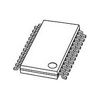
CBTD3384PW NXP Semiconductors, CBTD3384PW Datasheet - Page 3

CBTD3384PW
Manufacturer Part Number
CBTD3384PW
Description
Bus Switch 2-Element 5-IN 24-Pin TSSOP Tube
Manufacturer
NXP Semiconductors
Specifications of CBTD3384PW
Package
24TSSOP
Configuration
5 x 1:1
Logic Family
CBT
Logic Function
Bus Switch
Number Of Elements Per Chip
2
Number Of Outputs Per Chip
10
Typical Operating Supply Voltage
5 V
Maximum On Resistance
17(Typ) Ohm
Maximum High Level Output Current
-128 mA
Maximum Low Level Output Current
128 mA
Maximum Operating Supply Voltage
5.5 V
Minimum Operating Supply Voltage
4.5 V
Maximum Propagation Delay Time @ Maximum Cl
0.25@5V ns
Number Of Bits
10
Number Of Elements
2
Technology
CMOS
High Level Output Current
-128mA
Low Level Output Current
128mA
On Resistance
17Ohm
Propagation Delay Time
7ns
Package Type
TSSOP
Operating Temp Range
-40C to 85C
Operating Temperature Classification
Industrial
Operating Supply Voltage (min)
4.5V
Operating Supply Voltage (typ)
5V
Operating Supply Voltage (max)
5.5V
Quiescent Current
1.5mA
Pin Count
24
Mounting
Surface Mount
Lead Free Status / Rohs Status
Compliant
1. Stresses beyond those listed may cause permanent damage to the device. These are stress ratings only and functional operation of the
2. The performance capability of a high-performance integrated circuit in conjunction with its thermal environment can create junction
3. The input and output voltage ratings may be exceeded if the input and output current ratings are observed.
Philips Semiconductors
LOGIC SYMBOL
ABSOLUTE MAXIMUM RATINGS
NOTES:
RECOMMENDED OPERATING CONDITIONS
2001 Dec 20
SYMBOL
SYMBOL
SYMBOL
10-bit level shifting bus switch
with 5-bit output enables
device at these or any other conditions beyond those indicated under “recommended operating conditions” is not implied. Exposure to
absolute-maximum-rated conditions for extended periods may affect device reliability.
temperatures which are detrimental to reliability. The maximum junction temperature of this integrated circuit should not exceed 150 C.
T
V
V
I
T
V
V
I
SW
amb
V
CC
IK
stg
CC
IH
IL
I
DC supply voltage
DC input diode current
DC input voltage
DC output diode current
Storage temperature range
DC supply voltage
High-level input voltage
Low-level Input voltage
Operating free-air temperature range
1OE
2OE
1A1
1A5
2A1
2A5
11
14
22
13
3
1
PARAMETER
3
1, 2
10
15
23
SA00544
2
PARAMETER
PARAMETER
1B1
1B5
2B1
2B5
3
CONDITIONS
FUNCTION TABLE
H = High voltage level
L = Low voltage level
Z = High impedance “off ” state
V
O
1OE
< 0
H
H
L
L
INPUTS
2OE
H
H
L
L
Min
–40
4.5
2.0
—
LIMITS
–0.5 to +7.0
–1.2 to +7.0
–65 to +150
RATING
–50
1A = 1B
1A = 1B
128
1A, 1B
Z
Z
Max
+85
5.5
0.8
—
OUTPUTS
CBTD3384
2A = 2B
2A= 2B
2A, 2B
Product data
UNIT
UNIT
UNIT
Z
Z
mA
mA
V
V
V
V
V
C
C


