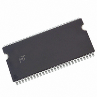
MT48LC64M8A2TG-75 IT:C Micron Technology Inc, MT48LC64M8A2TG-75 IT:C Datasheet - Page 64

MT48LC64M8A2TG-75 IT:C
Manufacturer Part Number
MT48LC64M8A2TG-75 IT:C
Description
DRAM Chip SDRAM 512M-Bit 64Mx8 3.3V 54-Pin TSOP-II Tray
Manufacturer
Micron Technology Inc
Type
SDRAMr
Datasheet
1.MT48LC64M8A2TG-75C_TR.pdf
(68 pages)
Specifications of MT48LC64M8A2TG-75 IT:C
Package
54TSOP-II
Density
512 Mb
Address Bus Width
15 Bit
Operating Supply Voltage
3.3 V
Maximum Clock Rate
133 MHz
Maximum Random Access Time
6|5.4 ns
Operating Temperature
-40 to 85 °C
Format - Memory
RAM
Memory Type
SDRAM
Memory Size
512M (64M x 8)
Speed
133MHz
Interface
Parallel
Voltage - Supply
3 V ~ 3.6 V
Package / Case
54-TSOP II
Lead Free Status / RoHS Status
Contains lead / RoHS non-compliant
Figure 48:
PDF: 09005aef809bf8f3/Source: 09005aef80818a4a
512MbSDRAM.fm - Rev. L 10/07 EN
DQML, DQMH
COMMAND
A11, A12
BA0, BA1
A0–A9,
DQM/
CLK
CKE
A10
DQ
t CMS
t CKS
t AS
t AS
t AS
ACTIVE
BANK
T0
ROW
ROW
Single WRITE with Auto Precharge
t CMH
t CKH
t AH
t AH
t AH
Notes:
t RCD 3
t RAS
t RC
t CK
T1
NOP 4
1. For this example, BL = 1, and the WRITE burst is followed by a “manual” PRECHARGE.
2. 14ns to 15ns is required between <D
3. x16: A11 and A12 = “Don’t Care”; x8: A12 = “Don’t Care.”
4. WRITE command not allowed else
quency.
t CL
NOP 4
T2
t CH
NOP 4
T3
ENABLE AUTO PRECHARGE
t CMS
t DS
COLUMN m
BANK
WRITE
T4
D
IN
t CMH
t DH
m
64
3
t WR
2
t
RAS would be violated.
IN
T5
NOP
m> and the PRECHARGE command, regardless of fre-
Micron Technology, Inc., reserves the right to change products or specifications without notice.
T6
NOP
t RP
512Mb: x4, x8, x16 SDRAM
T7
NOP
©2000 Micron Technology, Inc. All rights reserved.
Timing Diagrams
ACTIVE
ROW
ROW
BANK
T8
T9
NOP
Don’t Care
Undefined


