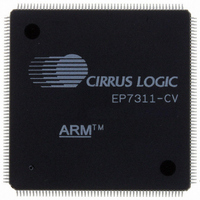
EP7311-CV Cirrus Logic Inc, EP7311-CV Datasheet - Page 47

EP7311-CV
Manufacturer Part Number
EP7311-CV
Description
Low-Power Processor 208-Pin LQFP
Manufacturer
Cirrus Logic Inc
Series
EP7r
Datasheet
1.EP7311-CV.pdf
(58 pages)
Specifications of EP7311-CV
Core Processor
ARM7
Core Size
32-Bit
Speed
74MHz
Connectivity
Codec, EBI/EMI, IrDA, Keypad, Multimedia Codec, SPI/Microwire1, UART/USART
Peripherals
LCD, LED, MaverickKey, PWM
Number Of I /o
27
Program Memory Type
ROMless
Ram Size
56K x 8
Voltage - Supply (vcc/vdd)
2.3 V ~ 2.7 V
Oscillator Type
External
Operating Temperature
0°C ~ 70°C
Package / Case
208-LQFP
Processor Series
EP73xx
Core
ARM720T
Data Bus Width
32 bit
3rd Party Development Tools
MDK-ARM, RL-ARM, ULINK2
Lead Free Status / RoHS Status
Contains lead / RoHS non-compliant
Eeprom Size
-
Program Memory Size
-
Data Converters
-
Lead Free Status / Rohs Status
No
Other names
598-1224
Available stocks
Company
Part Number
Manufacturer
Quantity
Price
Company:
Part Number:
EP7311-CV-90
Manufacturer:
Cirrus Logic Inc
Quantity:
10 000
DS506F1
Ball Location
F10
F11
F12
F13
F14
F15
F16
G10
G11
G12
G13
G14
G15
G16
H10
H11
H12
H13
H14
H15
H16
G1
G2
G3
G4
G5
G6
G7
G8
G9
F7
F8
F9
H1
H2
H3
H4
H5
H6
H7
H8
H9
J1
J2
J3
J4
J5
J6
Table V. 256-Ball PBGA Ball Listing (Continued)
A[13]/DRA[14]
nBATCHG
VSSRTC
VSSRTC
VSSRTC
VSSRTC
VSSRTC
VSSRTC
SDCKE
BATOK
VDDIO
VDDIO
VSSIO
VSSIO
VSSIO
VSSIO
VSSIO
TXD[1]
Name
DD[3]
DD[0]
D[11]
PB[1]
PB[4]
PB[6]
D[12]
D[13]
PA[7]
PA[5]
PA[4]
PA[6]
PB[0]
PB[2]
A[10]
A[11]
A[12]
D[14]
D[15]
PA[3]
PA[1]
PA[2]
PA[0]
TDO
A[1]
D[6]
D[3]
A[7]
A[8]
A[9]
Core ground Real time clock ground
RTC ground Real time clock ground
RTC ground Real time clock ground
RTC ground Real time clock ground
RTC ground Real time clock ground
RTC ground Real time clock ground
Pad ground I/O ground
Pad ground I/O ground
Pad ground I/O ground
Pad ground I/O ground
Pad ground I/O ground
Pad power
Pad power
Type
I/O
I/O
I/O
I/O
I/O
I/O
I/O
O
O
O
O
O
O
O
O
O
O
O
O
O
I
I
I
I
I
I
I
I
I
I
I
I
I
I
I
SDRAM clock enable output
LCD serial display data
System byte address
Data I/O
Battery ok input
Battery changed sense input
Data I/O
Digital I/O power, 3.3V
GPIO port B
Digital I/O power, 3.3V
JTAG data out
GPIO port B
GPIO port B
LCD serial display data
Data I/O
System byte address
System byte address
System byte address
Data I/O
Data I/O
GPIO port A
GPIO port A
GPIO port A
GPIO port A
GPIO port B
GPIO port B
System byte address
System byte address
System byte address
System byte address / SDRAM address
Data I/O
Data I/O
GPIO port A
GPIO port A
GPIO port A
GPIO port A
UART 1 transmit data out
Description
©
Copyright Cirrus Logic, Inc. 2005
(All Rights Reserved)
Ball Location
K10
K11
K12
K13
K14
K15
K16
L10
L11
L12
L13
L14
L15
L16
J10
J11
J12
J13
J14
J15
J16
M1
M2
M3
M4
M5
M6
J7
J8
J9
K1
K2
K3
K4
K5
K6
K7
K8
K9
L1
L2
L3
L4
L5
L6
L7
L8
L9
Table V. 256-Ball PBGA Ball Listing (Continued)
PE[0]/BOOTSEL[0]
PD[0]/LEDFLSH
High-Performance, Low-Power System on Chip
PE[2]/CLKSEL
A[17]/DRA[10]
A[16]/DRA[11]
A[15]/DRA[12]
A[14]/DRA[13]
A[22]/DRA[5]
A[21]/DRA[6]
A[18]/DRA[9]
A[19]/DRA[8]
nTEST[1]
nTEST[0]
VSSRTC
VSSRTC
LEDDRV
VSSRTC
nEINT[1]
VSSRTC
VSSRTC
VSSRTC
nEINT[2]
EINT[3]
nTRST
PHDIN
VSSIO
ADCIN
COL[4]
VSSIO
VDDIO
VDDIO
RXD[1]
VDDIO
COL[6]
VSSIO
VDDIO
VDDIO
Name
TCLK
D[16]
D[17]
D[20]
D[19]
D[18]
D[31]
DCD
DSR
TMS
CTS
RTC ground Real time clock ground
RTC ground Real time clock ground
RTC ground Real time clock ground
RTC ground Real time clock ground
Core ground Real time clock ground
RTC ground Real time clock ground
Pad ground I/O ground
Pad ground I/O ground
Pad ground I/O ground
Pad power
Pad power
Pad power
Pad power
Pad power
Type
I/O
I/O
I/O
I/O
I/O
I/O
I/O
O
O
O
O
O
O
O
O
O
O
O
I
I
I
I
I
I
I
I
I
I
I
I
I
I
I
I
UART 1 clear to send input
System byte address / SDRAM address
System byte address / SDRAM address
System byte address / SDRAM address
System byte address / SDRAM address
JTAG async reset input
Data I/O
Data I/O
IR LED drivet
Photodiode input
UART 1 data carrier detect
Test mode select input
External interrupt
SSI1 ADC serial input
Keyboard scanner column drive
JTAG clock
Data I/O
Data I/O
Data I/O
Digital I/O power, 3.3V
Digital I/O power, 3.3V
UART 1 receive data input
UART 1 data set ready input
Digital I/O power, 3.3V
External interrupt input
GPIO port E / clock input mode select
GPIO port D / LED blinker output
Keyboard scanner column drive
Data I/O
System byte address / SDRAM address
System byte address / SDRAM address
System byte address / SDRAM address
System byte address / SDRAM address
Test mode select input
External interrupt input
Digital I/O power, 3.3V
GPIO port E / Boot mode select
JTAG mode select
Digital I/O power, 3.3V
Description
EP7311
47


