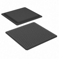
XC3S1400AN-5FGG676C Xilinx Inc, XC3S1400AN-5FGG676C Datasheet - Page 87

XC3S1400AN-5FGG676C
Manufacturer Part Number
XC3S1400AN-5FGG676C
Description
FPGA Spartan®-3AN Family 1.4M Gates 25344 Cells 770MHz 90nm Technology 1.2V 676-Pin FBGA
Manufacturer
Xilinx Inc
Series
Spartan™-3ANr
Datasheets
1.XC3S50A-4VQG100C.pdf
(7 pages)
2.XC3S50AN-4TQG144C.pdf
(2 pages)
3.XC3S50AN-4TQG144C.pdf
(123 pages)
Specifications of XC3S1400AN-5FGG676C
Package
676FBGA
Family Name
Spartan®-3AN
Device Logic Units
25344
Device System Gates
1400000
Maximum Internal Frequency
770 MHz
Typical Operating Supply Voltage
1.2 V
Maximum Number Of User I/os
502
Ram Bits
589824
Number Of Logic Elements/cells
25344
Number Of Labs/clbs
2816
Total Ram Bits
589824
Number Of I /o
502
Number Of Gates
1400000
Voltage - Supply
1.14 V ~ 1.26 V
Mounting Type
Surface Mount
Operating Temperature
0°C ~ 85°C
Package / Case
676-BBGA
Lead Free Status / RoHS Status
Lead free / RoHS Compliant
Other names
122-1600
XC3S1400AN-5FGG676C
XC3S1400AN-5FGG676C
Available stocks
Company
Part Number
Manufacturer
Quantity
Price
Company:
Part Number:
XC3S1400AN-5FGG676C
Manufacturer:
XILINX
Quantity:
490
Company:
Part Number:
XC3S1400AN-5FGG676C
Manufacturer:
Xilinx Inc
Quantity:
10 000
Footprint Migration Differences
Unconnected Balls on XC3S50AN
Table 73
XC3S400AN devices for migration between these devices in the FTG256 package. The XC3S200AN and XC3S400AN have
identical pinouts. The XC3S50AN pinout is compatible with the XC3S200AN and XC3S400AN, however, there are 51
unconnected balls and one functionally different ball. Generally, designs migrate upward from the XC3S50AN to either the
XC3S200AN or XC3S400AN. If using differential I/O, see
Table
In
right. Migration in the other direction is possible depending on how the pin is configured for the device on the right.
Table 73: FTG256 XC3S50AN Footprint Migration/Differences
DS557 (v4.1) April 1, 2011
Product Specification
Table
FTG256 Ball
75.
G13
G14
G16
A12
B12
D10
E10
E16
H13
F14
F15
F16
J10
J11
A7
C7
E2
E3
E7
G3
G4
G5
G6
H4
H5
H6
K4
F3
F8
J4
J6
73, the arrow () indicates that this pin can unconditionally migrate from the device on the left to the device on the
summarizes any footprint and functionality differences between the XC3S50AN and the XC3S200AN or
Bank
0
0
0
0
0
3
3
0
0
1
3
0
1
1
1
3
3
3
3
1
1
1
3
3
3
1
3
3
1
1
3
N.C.
N.C.
INPUT
N.C.
N.C.
N.C.
N.C.
N.C.
N.C.
N.C.
N.C.
N.C.
N.C.
N.C.
N.C.
N.C.
N.C.
N.C.
N.C.
N.C.
N.C.
N.C.
N.C.
N.C.
N.C.
N.C.
N.C.
N.C.
N.C.
N.C.
N.C.
XC3S50AN
www.xilinx.com
Table
74. If using the BPI configuration mode (parallel Flash), see
Spartan-3AN FPGA Family: Pinout Descriptions
Migration
I/O
I/O
I/O
I/O
I/O
I/O
I/O
I/O/VREF
I/O/VREF
I/O
I/O
I/O
I/O
I/O
I/O
I/O
I/O
INPUT/VREF
INPUT
I/O
I/O
I/O
I/O
I/O
I/O
I/O
I/O
I/O
INPUT/VREF
INPUT
I/O
XC3S200AN or XC3S400AN
87


